Cleaning agent for thick-film photoresist

A cleaning agent and photoresist technology, applied in the processing of photosensitive materials, etc., can solve the problems of insufficient cleaning ability, strong corrosion of semiconductor wafer patterns and substrates, etc., and achieve the effect of low etching rate

Inactive Publication Date: 2012-07-04
ANJI MICROELECTRONICS (SHANGHAI) CO LTD
View PDF7 Cites 13 Cited by
  • Summary
  • Abstract
  • Description
  • Claims
  • Application Information

AI Technical Summary

Problems solved by technology

[0006] The technical problem to be solved by the present invention is to provide a method for cleaning thick-film photoresist in view of the insufficient cleaning ability of existing thick-film photore

Method used


Image

  • Cleaning agent for thick-film photoresist
  • Cleaning agent for thick-film photoresist
  • Cleaning agent for thick-film photoresist

Examples


Embodiment Construction

[0012] The present invention will be further described below through specific embodiments.

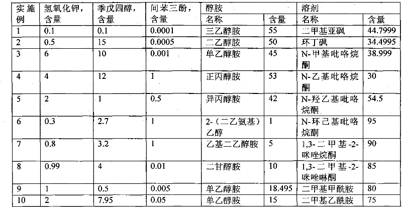
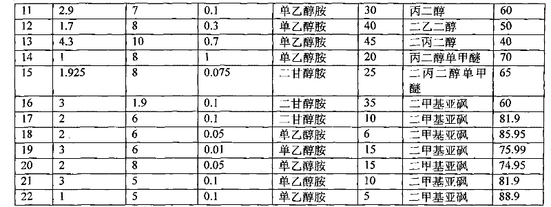
[0013] Component and content of cleaning agent in each embodiment (Examples) of table 1

[0014]

[0015]

[0016] Note: NA means that this component was not added.

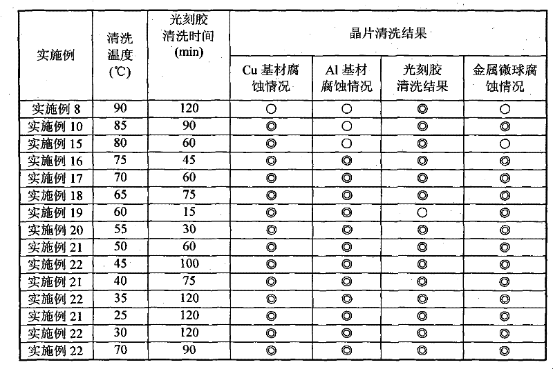
[0017] In order to further investigate the cleaning situation of this type of cleaning solution, the present invention adopts the following technical means: the semiconductor wafer (bump package) that will contain negative acrylic photoresist (thickness is about 120 microns, and through exposure and etching) (wafer) immersed in cleaning agent, vibrating with a constant temperature oscillator at a vibration frequency of about 60 rpm for 15 to 120 minutes at 25 to 90° C., then washed with deionized water and blown dry with high-purity nitrogen. The cleaning effect of the photoresist and the corrosion situation of the wafer by the cleaning solution are shown in Table 2.

[0018] Table 2 embodiment to wafer cleaning s...


PUM


Abstract

The invention discloses a cleaning agent suitable for cleaning thick photoresist and with low etching performance, which contains (a) potassium hydroxide, (b) dissolvent, (c) pentaerythritol, (d) alkylol amine and (e) phloroglucinol. The cleaning agent for the photoresist can also be used for removing the photoresist and other residues on metal, metal alloy or dielectric medium substrates, has low etch rate on metal including copper (Cu) and the like simultaneously, and has good application prospect in microelectronics fields including semiconductor chip cleaning and the like.

Description

technical field [0001] The invention relates to a thick-film photoresist cleaning agent. Background technique [0002] In the usual semiconductor manufacturing process, a photoresist mask is formed on the surface of silicon dioxide, Cu (copper) and other metals and low-k materials, and the pattern is transferred after exposure. After the required circuit pattern is obtained, the Before the next process, the residual photoresist needs to be stripped off. For example, in the wafer microsphere implantation process (bumping technology), photoresist is required to form a mask, and the mask also needs to be removed after microspheres are successfully implanted, but because the photoresist is relatively thick, it is often difficult to completely remove it. more difficult. The more common methods to improve the removal effect are to extend the soaking time, increase the soaking temperature and use more aggressive solutions, but this often causes corrosion of the wafer substrate an...

Claims


Application Information

Patent Timeline
IPC IPC(8): G03F7/42
Inventor 刘兵彭洪修孙广胜
Owner ANJI MICROELECTRONICS (SHANGHAI) CO LTD
Why Eureka
Try Eureka