Method for producing very-long wave indium arsenide (InAs)/gallium antimonide (GaSb) second class superlattice infrared detector material

An infrared detector and very long wave technology, which is applied in semiconductor devices, final product manufacturing, sustainable manufacturing/processing, etc., can solve the problems of difficult preparation of superlattice infrared detector materials, affecting material quality, and deteriorating interface quality, etc. Achieve the effect of avoiding interface quality deterioration, reducing dark current, and good optical properties

Inactive Publication Date: 2012-07-04
INST OF SEMICONDUCTORS - CHINESE ACAD OF SCI
View PDF2 Cites 16 Cited by
  • Summary
  • Abstract
  • Description
  • Claims
  • Application Information

AI Technical Summary

Problems solved by technology

[0003] However, the preparation of very long-wave InAs/GaSb type II superlattice infrared detector materials is very difficult, because the superlattice material whose absorption cut-off wavelength is in the very long-wave band generally needs to have a thickness of about 5nm for InAs in one period. While there is a 0.6% lattice

Method used


Image

  • Method for producing very-long wave indium arsenide (InAs)/gallium antimonide (GaSb) second class superlattice infrared detector material
  • Method for producing very-long wave indium arsenide (InAs)/gallium antimonide (GaSb) second class superlattice infrared detector material
  • Method for producing very-long wave indium arsenide (InAs)/gallium antimonide (GaSb) second class superlattice infrared detector material

Examples


Embodiment Construction

[0024] In order to make the object, technical solution and advantages of the present invention clearer, the present invention will be described in further detail below in conjunction with specific embodiments and with reference to the accompanying drawings.

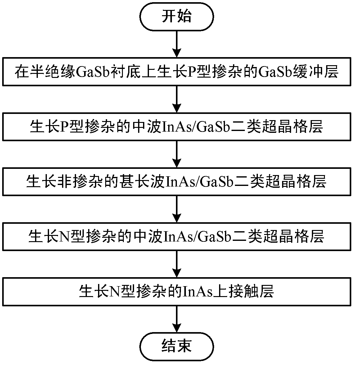
[0025] Such as figure 1 as shown, figure 1 It is a flow chart of a method for preparing a very long wave InAs / GaSb type II superlattice infrared detector material according to an embodiment of the present invention. The method uses a molecular beam epitaxy method and equipment to sequentially grow P-type doped materials on a semi-insulating GaSb substrate. Doped GaSb buffer layer, P-type doped medium wave InAs / GaSb type II superlattice layer, non-doped very long wave InAs / GaSb type II superlattice layer, N type doped medium wave InAs / GaSb type II superlattice layer The superlattice-like layer and the N-type doped InAs upper contact layer are used to obtain the very long-wave InAs / GaSb type II superlattice infrared detect...


PUM

PropertyMeasurementUnit
Thicknessaaaaaaaaaa
Thicknessaaaaaaaaaa

Abstract

The invention discloses a method for producing a very-long wave indium arsenide (InAs)/gallium antimonide (GaSb) second class superlattice infrared detector material, which comprises the step that: a P type doped GaSb buffer layer, a P type doped medium wave InAs/GaSb second class superlattice layer, a non-doped very-long wave InAs/GaSb second class superlattice layer, a N type doped medium wave InAs/GaSb second class superlattice layer and an N type doped InAs upper contact layer are sequentially grown on a semi-insulating GaSb substrate, so the very-long wave InAs/GaSb second class superlattice infrared detector material is obtained. After the method is utilized, because 'Sb-soak' and 'grow interruption' which are well designed are added in an interface design, the quality of the superlattice material is further improved.

Description

technical field [0001] The invention relates to the technical field of semiconductor infrared detection, in particular to a preparation method of a very long wave band (12-20 microns) InAs / GaSb type II superlattice infrared detector material. Background technique [0002] VLWIR detectors with a band of 12-20 microns have important applications in strategic early warning, atmospheric temperature and relative humidity profile detection, atmospheric small element distribution and space detection. Traditional mercury cadmium telluride detectors have excellent detection performance, but as the wavelength increases, the difficulty of its materials increases sharply, and it encounters great challenges in the very long wavelength band. Quantum well infrared detectors are easier to achieve very long-wavelength detection, but their quantum efficiency is low, and the performance of the device is limited to a certain extent. The second type of superlattice is an ideal very long wave de...

Claims


Application Information

Patent Timeline
IPC IPC(8): H01L31/18
CPCY02P70/50
Inventor 卫炀马文全张艳华曹玉莲
Owner INST OF SEMICONDUCTORS - CHINESE ACAD OF SCI
Why Eureka
Try Eureka