Method for doping silicon-based film by eutectic growth

A silicon-based film and surface normal technology, applied in ion implantation plating, metal material coating process, coating, etc., can solve the problems of high requirements for experimental equipment, many film defects, uneven distribution of doping elements, etc., to achieve The doping amount is easy to control, the content is uniform, and the effect of high doping concentration

Inactive Publication Date: 2012-07-11
GRADUATE SCHOOL OF THE CHINESE ACAD OF SCI GSCAS
View PDF3 Cites 6 Cited by
  • Summary
  • Abstract
  • Description
  • Claims
  • Application Information

AI Technical Summary

Problems solved by technology

Each of these methods has limitations
For example, in the ion implantation method, the dopant elements are unevenly distributed in the sample; the film prepared b

Method used


Image

  • Method for doping silicon-based film by eutectic growth
  • Method for doping silicon-based film by eutectic growth
  • Method for doping silicon-based film by eutectic growth

Examples


Example Embodiment

[0026] Embodiment one

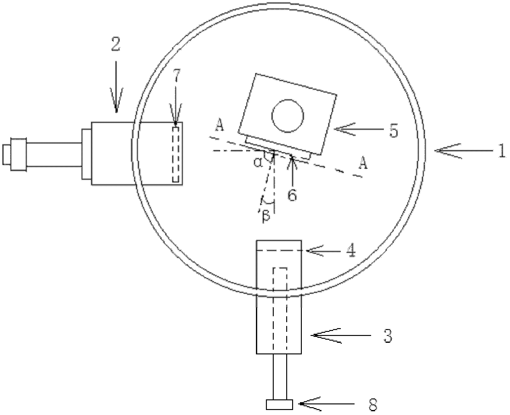
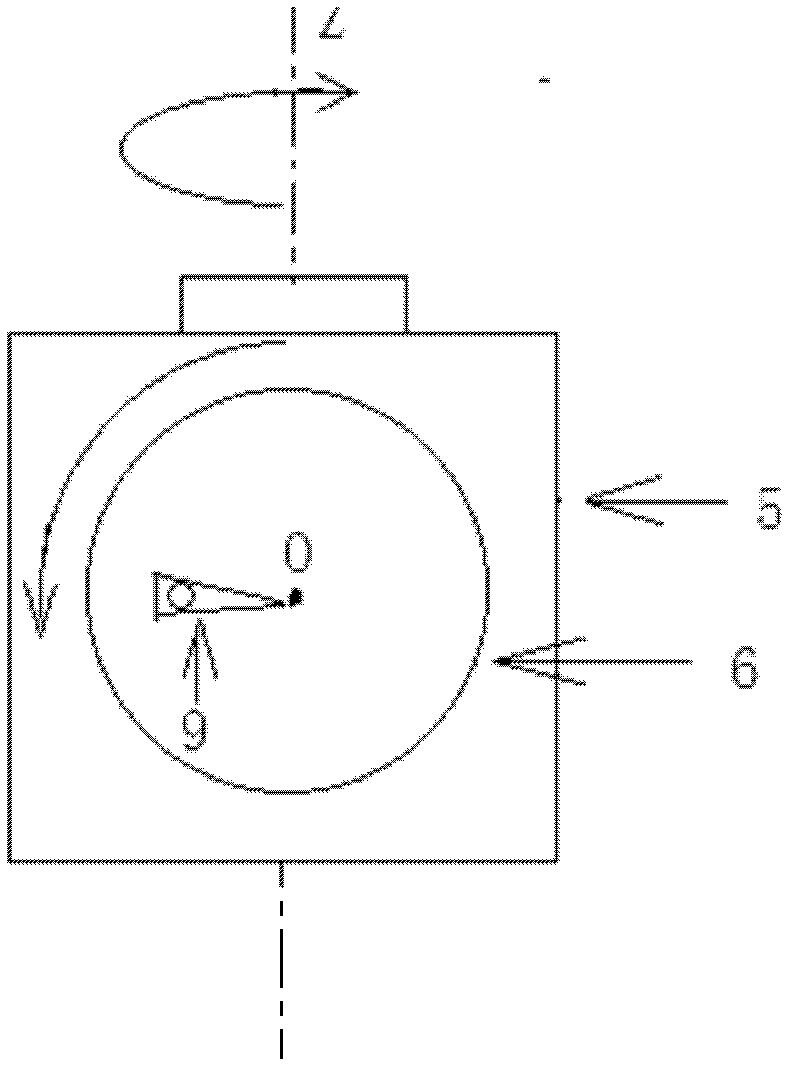
[0027] (1) The structure of the experimental device is as follows: figure 1 As shown, the distance between the hot wire source and the substrate is 8cm, the angle α=75 degrees between the normal line of the surface of the sample holder and the plane of the hot wire rack, and the sputtering target of the magnetron sputtering system has a purity of 99.995% titanium target;

[0028] (2) Put the cleaned substrate on the sample holder of the vacuum chamber so that the vacuum degree of the vacuum chamber is 3×10 -4 Pa;

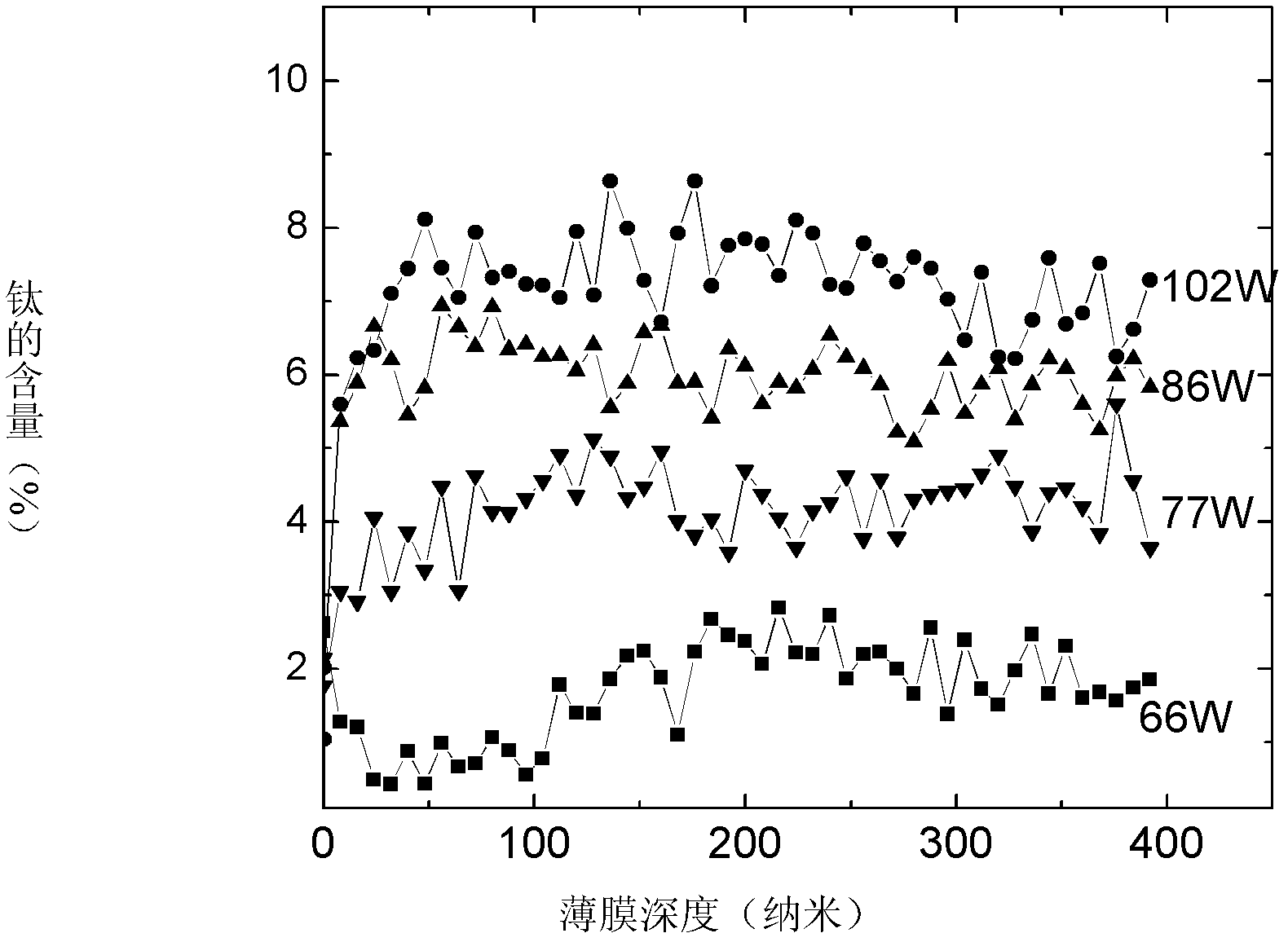
[0029] (3) feed reaction gas argon, hydrogen and silane in the vacuum chamber, the flow ratio of three kinds of gases is: hydrogen: argon: silane=12: 6: 6, make the air pressure of reaction gas in the cavity be 3 Pa, Heat the hot wire so that the temperature of the hot wire reaches 1800°C, apply a DC bias to the magnetron sputtering system, the power of the DC sputtering is 66 watts, and the rotation speed of the substrate holder relative ...

Example Embodiment

[0033] Embodiment two

[0034] (1) The structure of the experimental device is as follows: figure 1 As shown, the distance between the hot wire source and the substrate is 8cm, the angle α between the normal of the surface of the sample holder and the plane of the hot wire holder is α=85 degrees, and the sputtering target of the magnetron sputtering system has a purity of 99.995 % titanium target;

[0035] (2) Put the cleaned substrate on the sample holder of the vacuum chamber so that the vacuum degree of the vacuum chamber is 5×10 -4 Pa;

[0036] (3) feed reaction gas argon, hydrogen and silane in the vacuum chamber, the flow ratio of three kinds of gases is: argon: hydrogen: silane=16: 6: 9, make the air pressure of reaction gas in the chamber be 4 Pa, Heat the hot wire so that the temperature of the hot wire reaches 1700°C, apply a DC bias to the magnetron sputtering system, the power of the DC sputtering is 105 watts, and the rotation speed of the substrate holder rela...

Example Embodiment

[0039] Embodiment Three

[0040] (1) The structure of the experimental device is as follows: figure 1As shown, the distance between the hot wire source and the substrate is 8cm, the angle α between the normal of the sample holder surface and the plane of the hot wire holder is α=75 degrees, and the sputtering target of the magnetron sputtering system has a purity of 99.99% % silver target;

[0041] (2) Put the cleaned substrate on the sample holder of the vacuum chamber so that the vacuum degree of the vacuum chamber is 5×10 -4 Pa;

[0042] (3) feed reaction gas argon, hydrogen and silane in the vacuum chamber, the flow ratio of three kinds of gases is: argon: hydrogen: silane=8: 6: 6, make the air pressure of reaction gas in the chamber be 2 Pa, Heat the hot wire so that the temperature of the hot wire reaches 1700°C, apply a DC bias to the magnetron sputtering system, the power of the DC sputtering is 76 watts, and the rotation speed of the substrate holder relative to th...


PUM

PropertyMeasurementUnit
Thicknessaaaaaaaaaa

Abstract

The invention relates to a method for doping silicon-based film by eutectic growth, belonging to the technical field of film silicon materials. The method comprises the following steps of: firstly, arranging a hot filament chemical vapor deposition system and a magnetron sputtering system on the chamber body wall of a vacuum chamber; placing the cleaned substrate on a sample base of the vacuum chamber; introducing reactant gases, namely argon gas and hydrogen gas and silicane into the vacuum chamber; heating a hot filament; applying direct current bias to the magnetron sputtering system; and opening a baffle in front of a magnetron sputtering target and the hot filament to prepare the silicon-based film. Compared with the prior art, the method has the advantages that the content of doped elements in the prepared film is very uniform and mutant doping can be realized. In addition, the required equipment is simple, the doping ratio is easy to control and the film with high doping concentration and low ion damage can be prepared; and the method has the characteristics of convenience for operation, repeatability and reliability as well as broad application prospect.

Description

technical field [0001] The invention relates to a method for doping a silicon-based thin film through co-growth, and belongs to the technical field of preparation of thin-film silicon materials. Background technique [0002] In the research of silicon semiconductor materials, various doping of silicon materials is a very important process. Transition metal-doped dilute magnetic semiconductors, rare earth-doped hydrogenated amorphous silicon thin-film luminescent materials, and deep-level doped mid-band semiconductor materials are all research hotspots in recent years, and some fields require higher doping concentrations , far beyond the solid solubility of doping elements in silicon, so that they cannot be doped by traditional diffusion processes. At present, methods such as ion implantation, co-sputtering and metal-organic chemical vapor deposition (hereinafter referred to as MOCVD) are commonly used for metal doping of amorphous silicon and nanocrystalline silicon thin fi...

Claims


Application Information

Patent Timeline
IPC IPC(8): C23C14/35C23C14/16
Inventor 周玉荣刘丰珍
Owner GRADUATE SCHOOL OF THE CHINESE ACAD OF SCI GSCAS
Why Eureka
Try Eureka