
Gas sensing material of cuprous oxide and stannic oxide micro-nano heterogeneous medium array structure and preparing method thereof

An array structure, tin dioxide technology, applied in analytical materials, instruments, measuring devices, etc., can solve the problems of inability to prepare, unsatisfactory gas sensitivity, etc., achieve excellent gas sensitivity characteristics, improve temperature dependence, and high sensitivity Effect

Inactive Publication Date: 2014-12-10
JILIN UNIV
View PDF3 Cites 0 Cited by
  • Summary
  • Abstract
  • Description
  • Claims
  • Application Information

AI Technical Summary

Problems solved by technology

[0004] There are many preparation methods for these two semiconductor materials, including solid-phase method, precipitation method, sol-gel method and gas-phase chemical reaction method, etc., and the preparation methods of thin film materials mainly include sputtering method and CVD method, but these methods Can only synthesize Cu 2 O or SnO 2 Single oxide material, unable to prepare Cu 2 O and SnO 2 Gas-sensing materials with periodic ordered array structure of two oxides
And the gas-sensitivity of the gas-sensitive materials prepared by the above traditional test methods is not ideal at room temperature.

Method used


Image

  • Gas sensing material of cuprous oxide and stannic oxide micro-nano heterogeneous medium array structure and preparing method thereof
  • Gas sensing material of cuprous oxide and stannic oxide micro-nano heterogeneous medium array structure and preparing method thereof
  • Gas sensing material of cuprous oxide and stannic oxide micro-nano heterogeneous medium array structure and preparing method thereof

Examples


Embodiment 1

[0030] 1 Use deionized water, 0.004 moles of copper nitrate and 0.001 moles of stannous chloride to configure 50ml of electrolyte, and adjust the pH to 2.6 with nitric acid;

[0031] 2 In a temperature-controlled growth chamber, use the silicon wafer with surface oxidation treatment as the substrate, place the silicon wafer flat in the growth chamber, and then place two copper foil electrodes in parallel on the silicon wafer, and then drop the copper foil between the two electrodes electrolyte, and finally cover with a coverslip. Control the temperature at minus 4 degrees and leave it for 10 minutes;

[0032] 3 Then use the cooling element in the growth chamber to freeze the electrolyte, and naturally form a thin liquid layer of about 300 nanometers between the solidified electrolyte and the surface-oxidized substrate silicon wafer, and keep it at a low temperature of minus 4 degrees for 1 Hour;

[0033] 4 Apply a 2 Hz half-sine voltage (minimum voltage 0.4V, maximum voltage...

Embodiment 2

[0037] 1 Use deionized water, 0.004 moles of copper nitrate and 0.001 moles of stannous chloride to configure 50ml of electrolyte, and adjust the pH to 2.2 with nitric acid;

[0038] 2 In a temperature-controlled growth chamber, use the silicon wafer with surface oxidation treatment as the substrate, place the silicon wafer flat in the growth chamber, and then place two copper foil electrodes in parallel on the silicon wafer, and then drop the copper foil between the two electrodes electrolyte, and finally cover with a coverslip. Control the temperature at minus 2.6 degrees and place it for 20 minutes;

[0039] 3 Then use the cooling element in the growth chamber to freeze the electrolyte, and naturally form a thin liquid layer of about 300 nanometers between the solidified electrolyte and the surface-oxidized substrate silicon wafer, and keep it at a low temperature of minus 4 degrees for 1 Hour;

[0040] 4 Apply a 0.5Hz half-sine voltage (minimum voltage 0.4V, highest volt...

Embodiment 3

[0045] 1 Use deionized water, 0.0025 moles of copper nitrate and 0.0005 moles of stannous chloride to configure 50ml of electrolyte, and adjust the pH to 2.0 with nitric acid;

[0046] 2 In a temperature-controlled growth chamber, use the silicon wafer with surface oxidation treatment as the substrate, place the silicon wafer flat in the growth chamber, and then place two copper foil electrodes in parallel on the silicon wafer, and then drop the copper foil between the two electrodes electrolyte, and finally cover with a coverslip. Control the temperature at minus 2.6 degrees and leave it for 30 minutes;

[0047] 3 Then use the cooling element in the growth chamber to freeze the electrolyte, and naturally form a thin liquid layer of about 300 nanometers between the solidified electrolyte and the surface-oxidized substrate silicon wafer, and keep it at a low temperature of minus 4 degrees for 1 Hour;

[0048] 4 Apply a half-sine voltage of 0.2 Hz to the electrode (the lowest ...


PUM

PropertyMeasurementUnit
particle sizeaaaaaaaaaa

Abstract

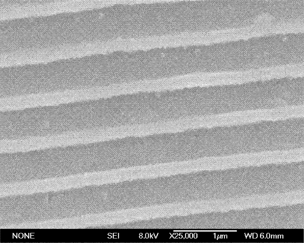
The invention relates to a gas sensing material of cuprous oxide and stannic oxide micro-nano heterogeneous medium array structure and a preparing method thereof, and belongs to the technical field related to gas sensing materials. The structure of the gas sensing material is a film material formed by periodically alternately assembling Cu2O and SnO2 which are parallel in elongated shapes, and the film material is generated on a silicon chip substrate, a Cu2O material is stacked thickly to form a protuberance portion, and a SnO2 material is stacked thinly to form a low ebb portion. The preparing method comprises parallelly placing two copper foil electrodes on a silicon substrate, dripping electrolyte prepared by copper nitrate and stannous chloride between the electrodes, covering a cover glass, refrigerating, solidifying and applying half-sine wave voltage, and enabling Cu2O and SnO2 to precipitate periodically and alternately. The gas sensing material of the heterogeneous medium array structure has gas sensing characteristics, the sensitivity of gas sensing elements is high at a room temperature because the gas sensing material has stable ordered heterogeneous medium structure, the service life is longe, simultaneously energy is saved and the environment is protected.

Description

technical field [0001] The invention belongs to the technical field related to gas-sensitive materials, and relates to Cu prepared by a quasi-two-dimensional electrochemical deposition method. 2 O and SnO 2 Related technologies of micro-nano heterogeneous array structure materials. Background technique [0002] Gas-sensitive materials have important applications in the monitoring, forecasting and automatic control of flammable, explosive, toxic and harmful gases. Gas-sensitive materials mainly refer to metal oxide semiconductor materials. These materials are mainly surface-controlled gas-sensitive materials. After the gas to be measured is adsorbed on the surface of the material, a redox reaction occurs on the surface, thereby causing changes in electrical characteristics. The sensitivity of the gas sensor is affected by the adsorption and active sites as well as the working temperature. The particle size of gas-sensitive materials has a significant impact on the sensitiv...

Claims


Application Information

Patent Timeline
Patent Type & Authority Patents(China)
IPC IPC(8): G01N33/00
Inventor 张明喆崔光亮
Owner JILIN UNIV
Learn More