Radiation hardening material with insulation buried layer and preparation method of radiation hardening material
A technology of insulating buried layer and radiation reinforcement, which is applied in the manufacture of semiconductor/solid-state devices, electrical components, circuits, etc., can solve problems that affect the performance of devices or circuits, are difficult to recover, and the uniformity of nanocrystal distribution in the longitudinal direction is difficult to accurately control, etc., to achieve Avoid injection damage and achieve precise control of the effect
- Summary
- Abstract
- Description
- Claims
- Application Information
AI Technical Summary
Problems solved by technology
Method used
Image

Examples
Embodiment 1
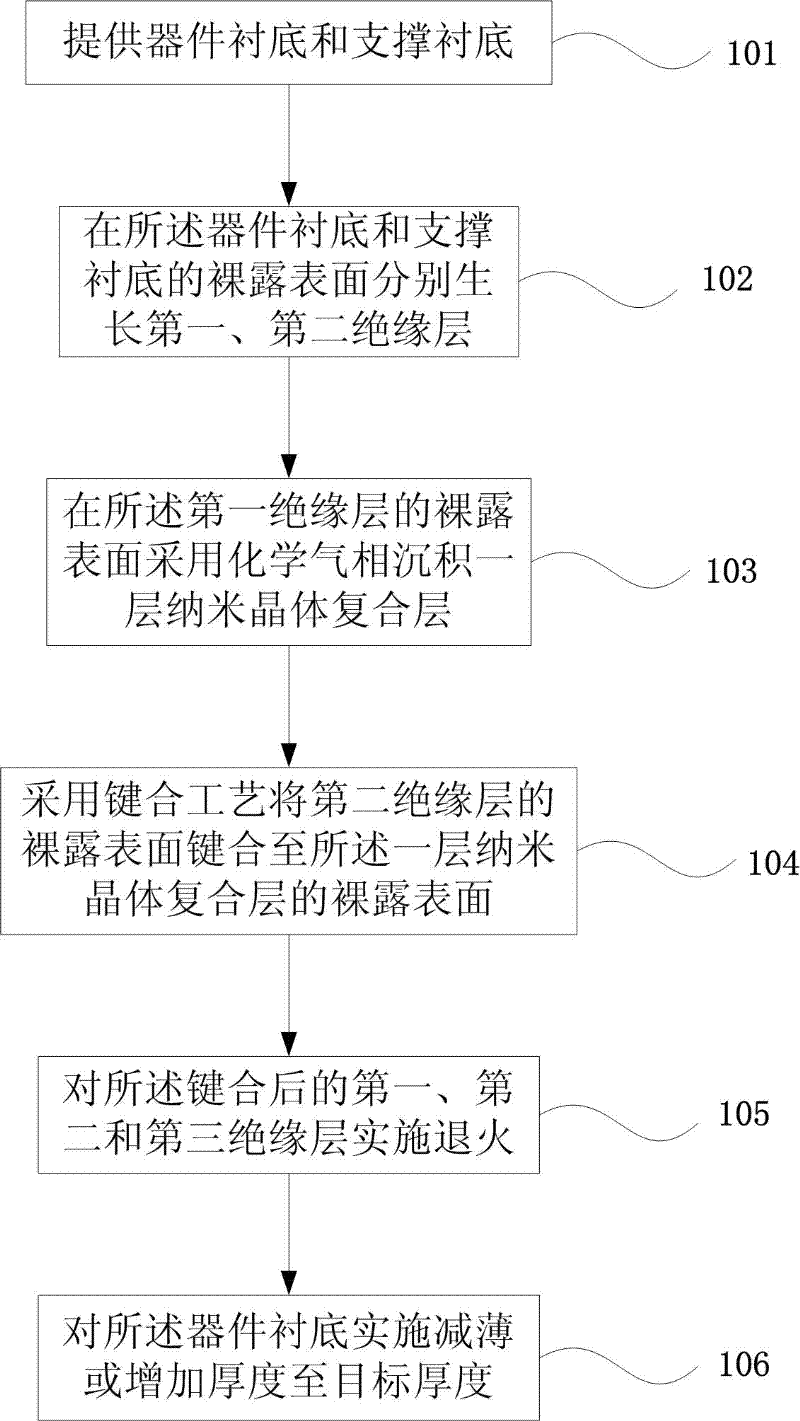
[0032] figure 1 Shown is a flow chart of the steps of Embodiment 1 of the preparation method of a radiation-reinforced material with an insulating buried layer provided by the present invention.
[0033] This embodiment provides a method for preparing a radiation-reinforced material with an insulating buried layer, including: step 101, providing a device substrate and a supporting substrate; step 102, forming a growing the first and second insulating layers respectively; step 103, depositing a nanocrystal composite layer on the exposed surface of the first insulating layer by chemical vapor phase; step 104, bonding the exposed surface of the second insulating layer to bonded to the exposed surface of the one nanocrystal composite layer; step 105, annealing the bonded first, second and third insulating layers; step 106, thinning or Increase thickness to target thickness.
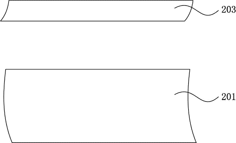
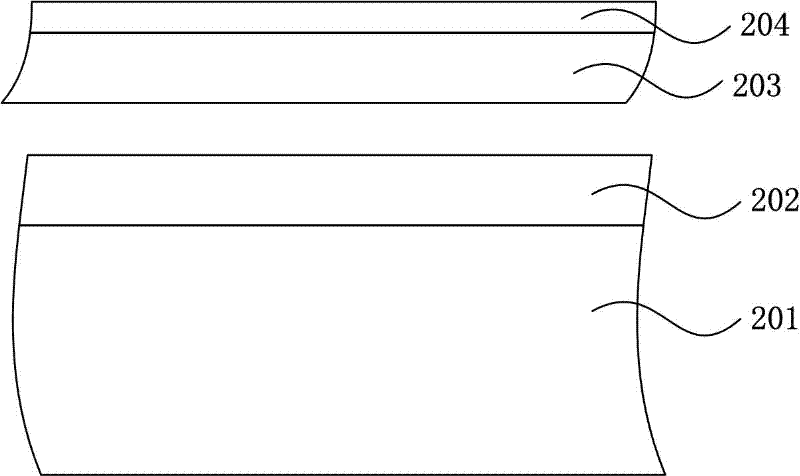
[0034] Figure 2A-2D Shown is a process flow chart of Embodiment 1 of the preparation method of a radia...
Embodiment 2
[0053] This embodiment provides a radiation-reinforced material with an insulating buried layer, the structure of which is as follows Figure 2D As shown, it is prepared by a bonding process, including a device substrate 201, an insulating buried layer and a supporting substrate 203 in sequence. The insulating buried layer includes a layer of nanocrystal composite layer placed in the insulating buried layer, and the nano The crystal composite layer sequentially includes a nanocrystal layer 206 and a third insulating layer 205, and the nanocrystal composite layer is formed by chemical vapor deposition, and the interface between the nanocrystal layer 206 and the first insulating layer 202 It is a bonding interface, and the interface between the nanocrystal layer 206 and the second insulating layer 204 is a bonding interface; the insulating buried layer further includes a first insulating layer 202, placed between the device substrate 201 and the layer Between the nanocrystal com...
PUM
| Property | Measurement | Unit |
|---|---|---|
| Thickness | aaaaa | aaaaa |
Abstract
Description
Claims
Application Information