
P-type high-concentration doped silicon and technology for preparing P-channel MOS (Metal Oxide Semiconductor) pipe of BCD products

A MOS tube and manufacturing process technology, applied in the field of semiconductor chip manufacturing process, can solve problems such as lattice defects and leakage, and achieve the effect of reducing the possibility of leakage, slowing impact, and reducing impact

Active Publication Date: 2014-04-16
FOUNDER MICROELECTRONICS INT
View PDF3 Cites 0 Cited by
  • Summary
  • Abstract
  • Description
  • Claims
  • Application Information

AI Technical Summary

Problems solved by technology

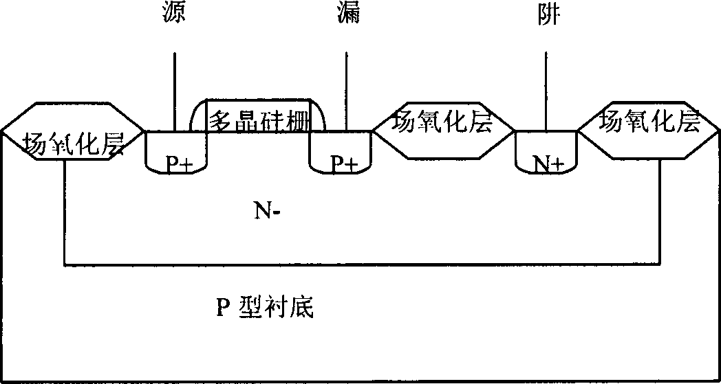
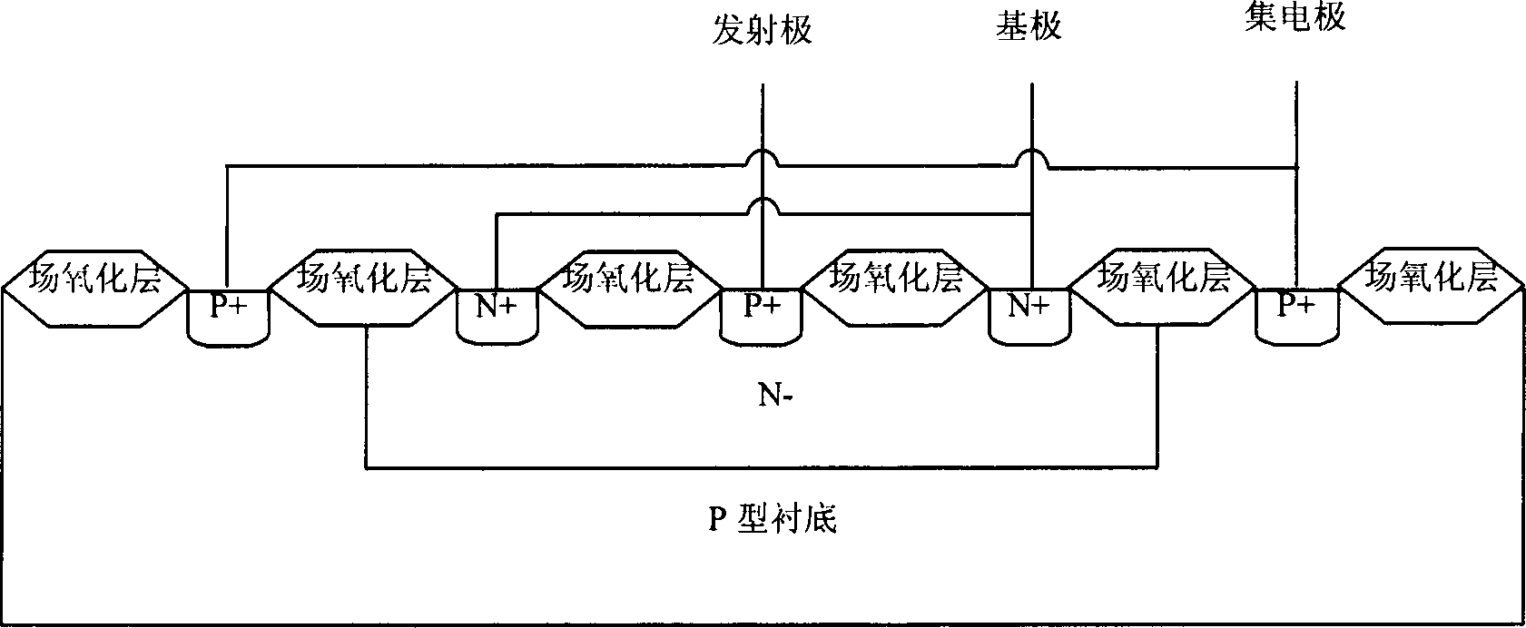
[0007] In view of this, the embodiment of the present invention provides a P-type high-concentration doped silicon and a BCD product P-channel MOS tube manufacturing process to solve the problem of P-type high-concentration doped silicon produced in the prior art due to lattice defects. Leakage problem

Method used


Image

  • P-type high-concentration doped silicon and technology for preparing P-channel MOS (Metal Oxide Semiconductor) pipe of BCD products
  • P-type high-concentration doped silicon and technology for preparing P-channel MOS (Metal Oxide Semiconductor) pipe of BCD products
  • P-type high-concentration doped silicon and technology for preparing P-channel MOS (Metal Oxide Semiconductor) pipe of BCD products

Examples


Embodiment Construction

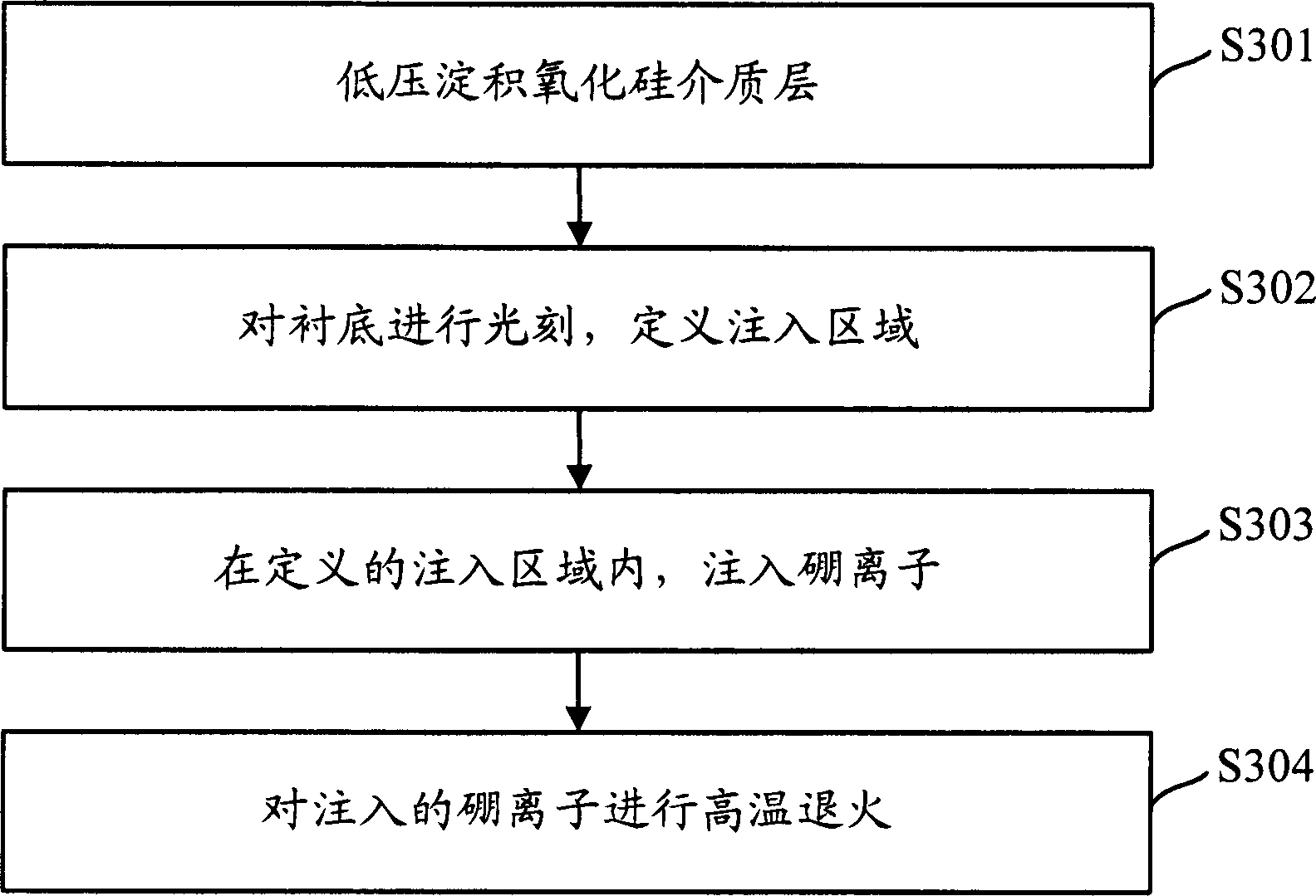
[0029] In order to effectively reduce the leakage problem in BCD products, the embodiment of the present invention provides a process realization method of P-type high-concentration doped silicon. In this step, an implantation region is defined, boron ions are implanted in the defined implantation region, and high-temperature annealing is performed on the implanted boron ions. Since the silicon oxide dielectric layer is deposited at a low pressure before the P-type high-concentration doped silicon is produced in the embodiment of the present invention, the impact of boron ion implantation on the silicon surface can be greatly reduced, and at the same time, the boron ion implantation energy can be controlled within achievable equipment and Within the range of process capability, on the other hand, during ion implantation, boron ions are implanted. Since the molecular weight of boron ions is relatively small, the implanted energy is relatively small, and the impact on the silicon...


PUM

PropertyMeasurementUnit
thicknessaaaaaaaaaa

Abstract

The invention discloses P-type high-concentration doped silicon and a technology for preparing a P-channel MOS (Metal Oxide Semiconductor) pipe of a BCD (Bipolar, Complementary Metal-Oxide-Semiconductor and Double-Diffusion Metal-Oxide-Semiconductor ) products, aiming at solving the problem of electricity leakage resulting from a lattice defect of the P-type high-concentration doped silicon manufactured with the prior art. A realization method of the technology of the P-type high-concentration doped silicon comprises the steps of conducting low-pressure deposition to form a silicon oxide dielectric layer, photoetching a substrate, defining an injection area, injecting boron ions in the defined injection area and conducting high-temperature annealing on the injected boron ions. According to the embodiment of the invention, before the P-type high-concentration doped silicon is prepared, the impact of the injection of the boron ions onto the surface of the silicon can be relieved by the low pressure deposition of the silicon oxide dielectric layer; the boron ions are injected when iron injection is conducted; as the molecular weight of the boron ions is smaller, the injected energy is smaller and the impact to the surface of the silicon is reduced; and in addition, as the injected impurities do not contain fluorine atoms, the defect problems caused by the fluorine atoms are avoided, and thus, the risk of generating the lattice defect is reduced and the probability of electricity leakage is lowered.

Description

technical field [0001] The invention relates to the technical field of semiconductor chip manufacturing technology, in particular to a P-type high-concentration doped silicon and a BCD product P-channel MOS transistor manufacturing technology. Background technique [0002] Silicon that does not contain impurities is called intrinsic silicon. Doping specific impurities in intrinsic silicon can form N-type silicon or P-type silicon that exhibits conductive characteristics. Specifically, doping group V elements into intrinsic silicon (such as phosphorus, arsenic, and antimony) can form N-type silicon, and doping III-group elements (such as boron) into intrinsic silicon can form P-type silicon. The industry uniformly stipulates that highly doped N-type silicon or P-type silicon is represented by a positive sign, and low-concentration doped N-type silicon or P-type silicon is represented by a negative sign. In the unsaturated condition, the higher the doping concentration in sil...

Claims


Application Information

Patent Timeline
Patent Type & Authority Patents(China)
IPC IPC(8): G02F1/1368H01L21/336H01L21/265H01L21/20
Inventor 潘光燃
Owner FOUNDER MICROELECTRONICS INT
Learn More