

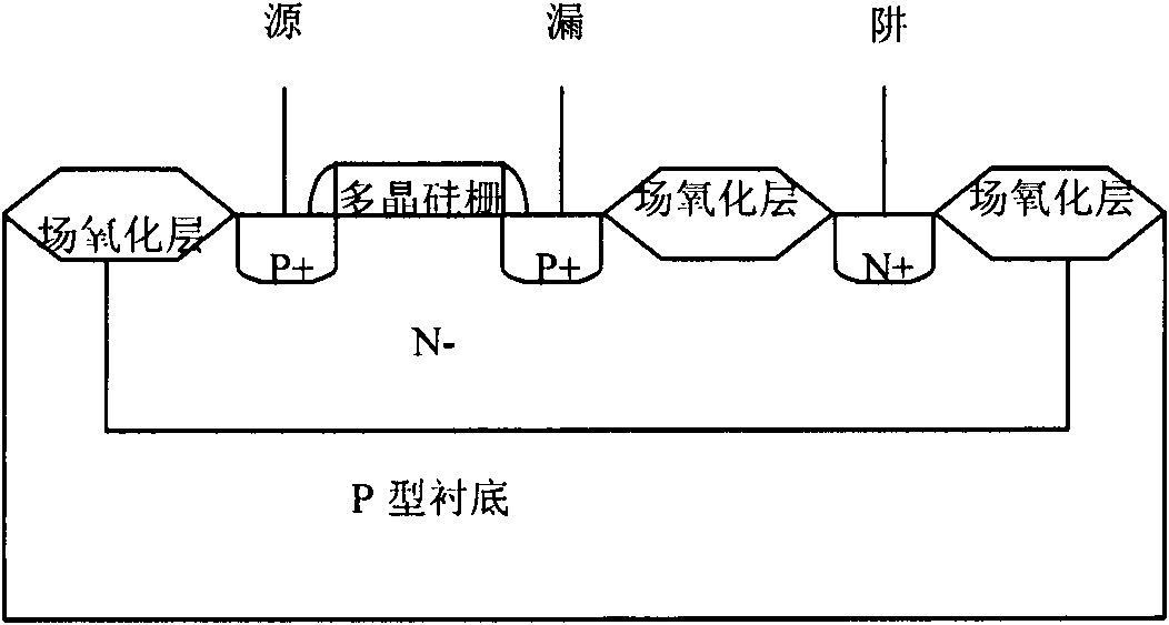
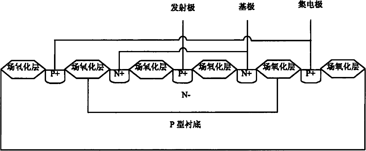
P-type high-concentration doped silicon and technology for preparing P-channel MOS (Metal Oxide Semiconductor) pipe of BCD (Bipolar, Complementary Metal-Oxide-Semiconductor and Double-Diffusion Metal-Oxide-Semiconductor) products
A manufacturing process and high-concentration technology, applied in semiconductor/solid-state device manufacturing, electrical components, circuits, etc., can solve problems such as lattice defects and leakage, reduce the possibility of leakage, slow down impact, and reduce lattice The effect of the risk of defects
- Summary
- Abstract
- Description
- Claims
- Application Information
AI Technical Summary
Problems solved by technology
Method used
Image

Examples
Embodiment Construction
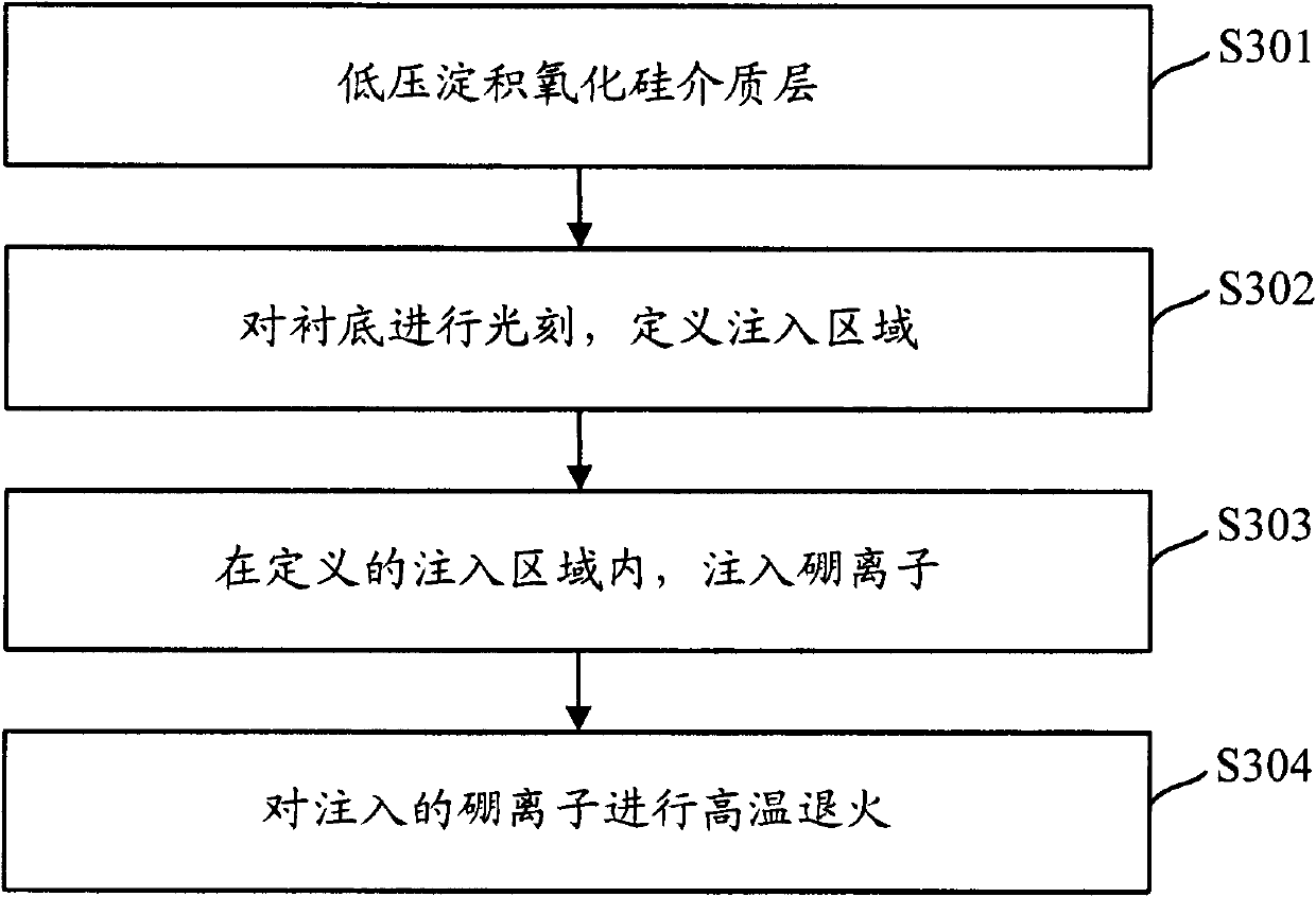
[0034] In order to effectively reduce the leakage problem in BCD products, the embodiment of the present invention provides a process realization method of P-type high-concentration doped silicon. In this step, an implantation region is defined, boron ions are implanted in the defined implantation region, and high-temperature annealing is performed on the implanted boron ions. Since the silicon oxide dielectric layer is deposited at a low pressure before the P-type high-concentration doped silicon is produced in the embodiment of the present invention, the impact of boron ion implantation on the silicon surface can be greatly reduced, and at the same time, the boron ion implantation energy can be controlled within achievable equipment and Within the range of process capability, on the other hand, during ion implantation, boron ions are implanted. Since the molecular weight of boron ions is relatively small, the implanted energy is relatively small, and the impact on the silicon...
PUM
| Property | Measurement | Unit |
|---|---|---|
| thickness | aaaaa | aaaaa |
Abstract
Description
Claims
Application Information