Method for cutting table facet silicon rectifying component

A cutting method and silicon rectification technology, which are applied to fine working devices, stone processing equipment, manufacturing tools, etc., can solve the problems of debris contamination of cutting width, easy edge collapse on both sides, and micro-damage, etc., and achieve smooth groove bottom. , the effect of eliminating micro-crack defects and improving performance

Active Publication Date: 2012-07-18
YANGZHOU HY TECH DEV
View PDF5 Cites 4 Cited by
  • Summary
  • Abstract
  • Description
  • Claims
  • Application Information

AI Technical Summary

Problems solved by technology

[0006] The technical problem to be solved by the present invention is to provide a cutting method for mesa silicon rectifier devices, which overcomes the high-speed rotary cutting of the traditional diamond grinding wheel, which causes easy edge chipping, micro damage, and cracks on the front and back sides, and at the same time causes debris pollution and narrower cutting widths. major defects

Method used


Image

  • Method for cutting table facet silicon rectifying component

Examples


Embodiment Construction

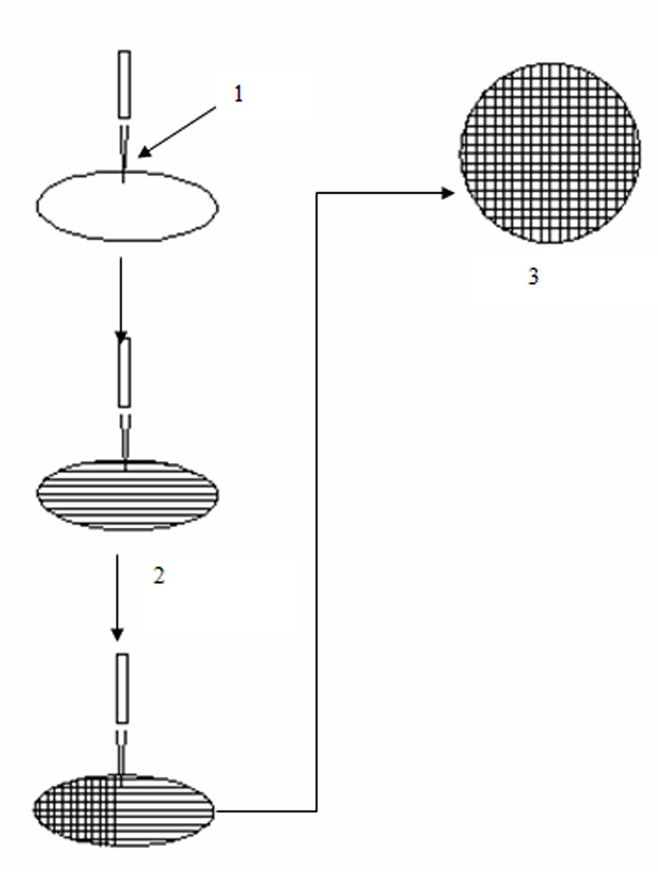
[0027] The principles and features of the present invention are described below in conjunction with the accompanying drawings, and the examples given are only used to explain the present invention, and are not intended to limit the scope of the present invention.

[0028] The specific operation steps for preparing a mesa silicon rectifier device:

[0029] (1) Perform phosphorus-boron diffusion at a high temperature of 1250±5°C on an N-type single crystal silicon wafer with a thickness of 280-290 μm and a resistivity of 30-40Ω·cm to form a silicon wafer with a PN junction.

[0030] (2) Carry out 1120 ± 5 ℃ oxidation to above-mentioned silicon chip, after forming oxide layer, use rotary gluing machine to drop 2-3ml negative photoresist on the surface of silicon chip, make the surface of silicon chip be coated with a layer of photoresist. Protective layer of engraving.

[0031] (3) After installing and aligning a photoresist plate on the upper and lower plates of the lithography...


PUM

PropertyMeasurementUnit
thicknessaaaaaaaaaa
electrical resistivityaaaaaaaaaa
wavelengthaaaaaaaaaa

Abstract

The invention relates to a method for cutting a table facet silicon rectifying component. The method comprises the following steps: oxidizing a silicon wafer diffused by phosphorus boron, carrying out double surface lithography on the silicon wafer, corroding the silicon wafer by using a mixed acid to obtain a PN junction table facet, cleaning and carrying out glass passivation, removing an oxidation layer on the surface of the silicon wafer by using a sand blasting method, performing chemical nickel-plating on the silicon wafer, sintering, forming good ohmic contact on the surface of the silicon wafer, cutting the silicon wafer by using a laser cutting machine, putting the silicon wafer on a slide holder with the back surface of the silicon wafer facing downwards, aligning, starting equipment, cutting, and manually cracking the silicon wafer to form single crystals. The process can effectively overcome the defect of the occurrence of microcracks of glass passivated chips caused by using the traditional grinding wheel cutting method, thereby improving the performances of a semiconductor device, and particularly improving the stability, the reliability and the compressive strength of a high back-pressure device.

Description

technical field [0001] The invention relates to a cutting method of a rectifying device, in particular to a cutting method of a mesa silicon rectifying device. Background technique [0002] The traditional diamond grinding wheel rotates at high speed for cutting, and the raised sharp serrated high-hardness diamond particles inlaid on the surface grind the cutting part, generating pressure, friction and shearing force to take away the peeled debris. The more blunt the blade, the higher the cutting temperature, which will cause the scribing knife to overload. Because these mechanical forces act directly on the wafer surface and generate stress and thermal damage inside the crystal, it is easy to cause chipping, micro damage, cracks and other problems on both sides, and at the same time cause debris pollution (Silicon dust ). The above problems are difficult to completely solve through the improvement of its own technology. [0003] With the increase of device integration, t...

Claims


Application Information

Patent Timeline
Patent Type & Authority Applications(China)
IPC IPC(8): B28D5/04
Inventor 王道强周红艳方文杰
Owner YANGZHOU HY TECH DEV
Why Eureka
Try Eureka