Method for adjusting diameter of silicon nanometer hole
A technology of pore size adjustment and silicon nano-technology, which is applied in the process of producing decorative surface effects, decorative art, gaseous chemical plating, etc., can solve the problems of large hole size deviation, waste of nano-optical devices, poor flexibility, etc., to achieve The effect of meeting the design requirements
- Summary
- Abstract
- Description
- Claims
- Application Information
AI Technical Summary
Problems solved by technology
Method used
Image
Examples
Embodiment 1
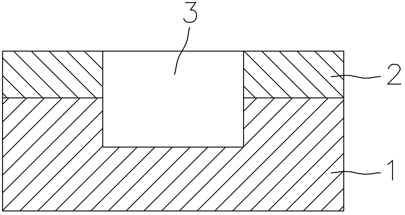
[0039] first step, such as figure 1 As shown, a layer of electron beam photoresist 2 is spin-coated on the front side of a silicon substrate 1 with a thickness of 500 microns. The positive resist ZEP-520A was selected as the electron beam photoresist 2, and the resist was spun for 60 seconds at a rotational speed of 4000 rpm, and the thickness of the resist was measured to be 300 nm.
[0040] In the second step, a pattern of circular holes with a diameter of 200 nm is designed, and an electron beam exposure device is used to expose the pattern of circular holes on the photoresist 2 . Electron beam acceleration voltage is 100KV, exposure dose is 270μC / cm 2 . Then put the silicon substrate 1 together with the photoresist 2 into the developer solution "Amyl Acetate" for 2 minutes, and then put it into IPA for fixing for 1 minute.
[0041] In the third step, the pattern on the photoresist 2 is transferred to the silicon substrate 1 by etching, and the remaining photoresist 2 is...
Embodiment 2
[0058] The first step, with embodiment 1
[0059] The second step is to design a circular hole layout with a diameter of 300nm, and use electron beam exposure equipment to expose the circular hole pattern on the photoresist. Electron beam acceleration voltage is 100KV, exposure dose is 240μC / cm 2 . Then put the silicon substrate 1 together with the photoresist 2 into the developer solution "Amyl Acetate" for 2 minutes, and then put it into IPA for fixing for 1 minute.
[0060] The 3rd step, with embodiment 1
[0061] The fourth step is to measure the size of the prepared silicon nanoholes through an electron microscope. The measured diameter D1 of the silicon nanoholes is 230nm, and the expected value D2 is 300nm. At this time, D2>D1, Δ=D2-D1=70nm.
[0062] In the fifth step, the silicon substrate 1 is put into a high temperature oxidation furnace for oxidation. Dry oxidation was carried out in an oxygen atmosphere at 1000°C. According to the Dill-Grove model, the control...
Embodiment 3
[0066] The first step is to measure the size of the prepared silicon nanoholes through an electron microscope. The measured diameter D1 of the silicon nanoholes is 280nm, and the expected value D2 is 200nm. At this time, D1>D2, Δ=D1-D2=80nm.
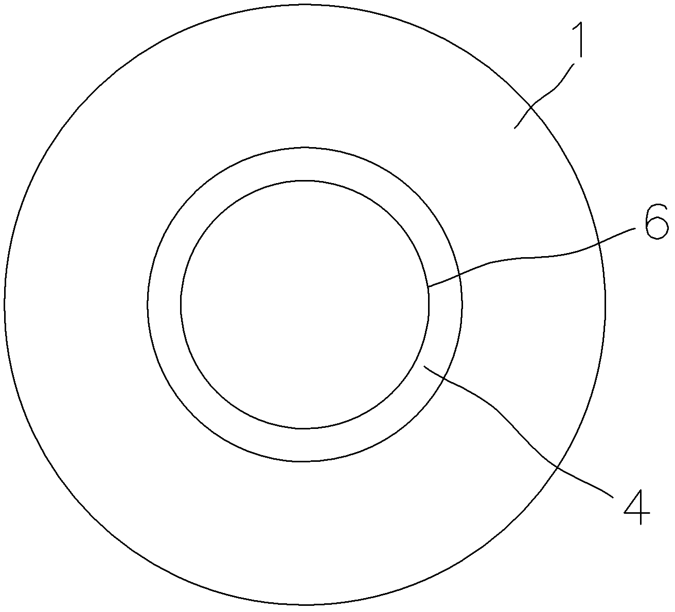
[0067] In the second step, put the silicon substrate 1 into a high temperature oxidation furnace for oxidation. Dry oxidation was carried out in an oxygen atmosphere at 1000°C. According to the Dill-Grove model, the control oxidation time is 1 hour and 50 minutes, at this time figure 2 The thickness of the silicon layer 4 consumed by thermal oxidation is r=31nm, ie: r=(Δ / 2)×(44 / 56)=(80 / 2)×(44 / 56)=31nm.
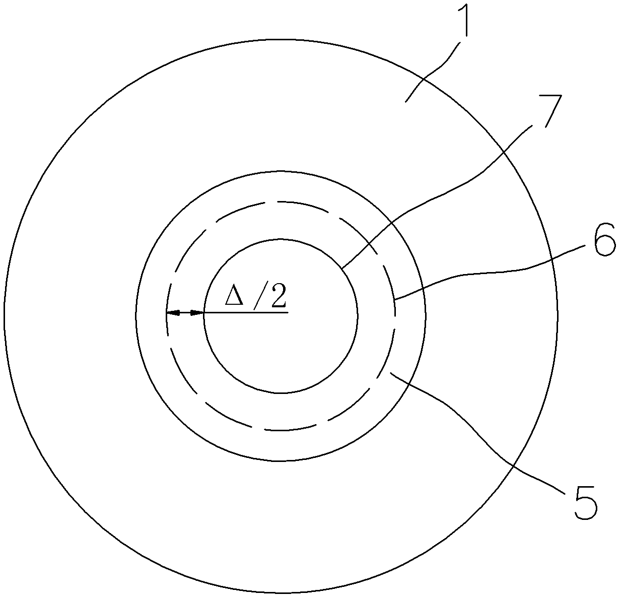
[0068] After the thermal oxidation is completed, it is obtained as image 3 The silicon dioxide layer 5 generated by thermal oxidation shown in . The silicon dioxide layer 5 generated by thermal oxidation makes the silicon nanopore extend from the boundary 6 of the original hole before thermal oxidation to the inside of the hole by Δ...
PUM
| Property | Measurement | Unit |
|---|---|---|
| thickness | aaaaa | aaaaa |
Abstract
Description
Claims
Application Information


