Device and method for large-area nano imprinting photoetching

It is a nano-imprinting and large-area technology, which is applied in the direction of photolithography, optics, and optomechanical equipment on the patterned surface. It can solve the problems of short working life, low elastic modulus, and substrate fracture, and simplify mold manufacturing. And embossing process, long working life, easy demoulding effect

Active Publication Date: 2012-07-18
QINGDAO TECHNOLOGICAL UNIVERSITY
View PDF6 Cites 31 Cited by
  • Summary
  • Abstract
  • Description
  • Claims
  • Application Information

AI Technical Summary

Problems solved by technology

At present, there are two main processes for realizing single-step whole wafer nanoimprint lithography: the whole wafer hot embossing process using a hard mold, but this method has high requirements for the flatness and hardness of the substrate. Not suitable for imprinting of non-flat (bent, warped or stepped), curved substrates and fragile substrates (such as LED patterning)
The second method is soft ultraviolet nanoimprinting based on PDMS, but the elastic modulus of PDMS is low, and the large imprinting force in the process of large-area imprinting is easy to cause deformation, poor wear resistance, and very short working life. PDMS also has a big disadvantage: in organic solvents, it has problems with swelling (Swell) and deformation, which seriously affects the accuracy of embossed graphics and mold life
However, epitaxial growth will lead to more obvious bending of large-scale substrates. In the subsequent lithography process, forced use of vacuum adsorption and other methods to compensate for this bending in exchange for high resolution in lithography may cause substrate breakage.

Method used


Image

  • Device and method for large-area nano imprinting photoetching
  • Device and method for large-area nano imprinting photoetching
  • Device and method for large-area nano imprinting photoetching

Examples


Embodiment Construction

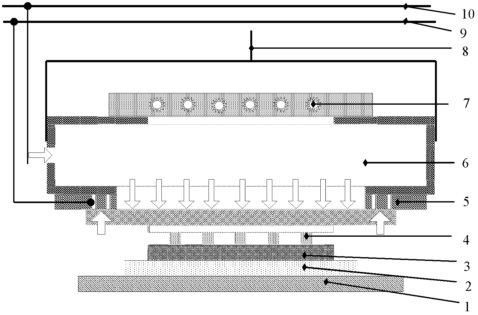
[0050] The present invention will be described in further detail below in conjunction with the accompanying drawings and embodiments.

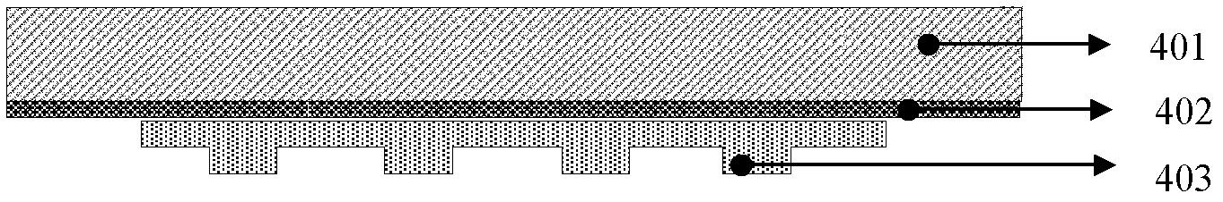
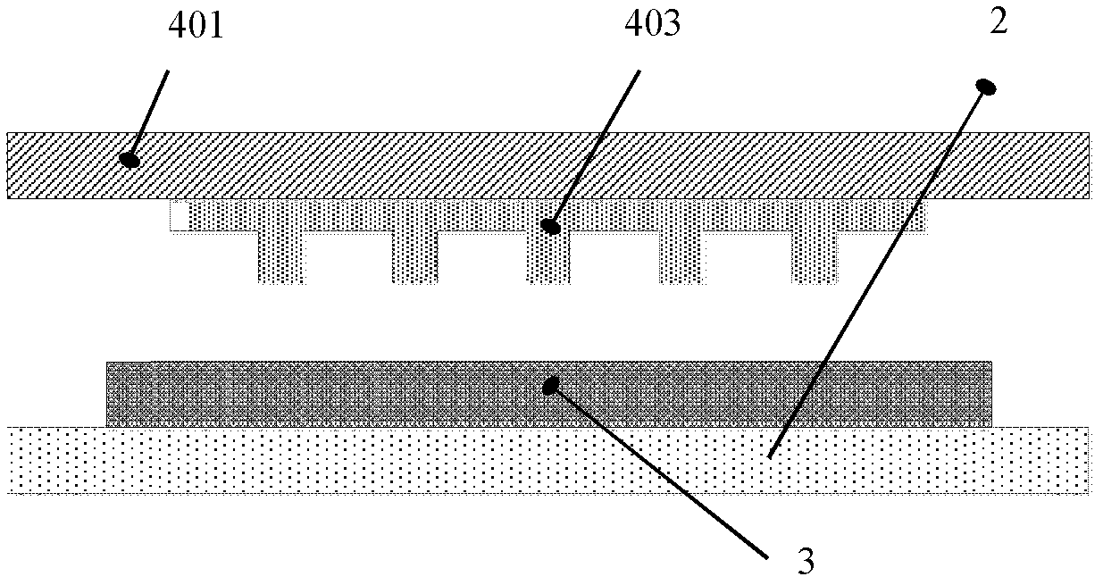
[0051] figure 1 Among them, it includes: workbench 1, substrate (wafer, epitaxial wafer) 2, liquid organic polymer 3, template 4, gas valve plate 5, gas chamber 6, ultraviolet light source 7, imprinting mechanism 8, vacuum tube Road 9, pressure pipeline 10; wherein, the whole wafer substrate 2 coated with liquid organic polymer 3 is fixed on the workbench 1; the template 4 is adsorbed on the bottom surface of the valve plate 5 through the vacuum pipeline 9 (template 4 The outermost side is adhered to the valve plate 5 to ensure that when there is no vacuum suction adsorption, the mold is still sealed with the valve plate 5), the valve plate 5 is fixed on the bottom surface of the air chamber 6, and the ultraviolet light source LED lamp array 7 is fixed On the top surface of the air chamber 6 ; the embossing mechanism 8 is connected to the air...


PUM

PropertyMeasurementUnit
thicknessaaaaaaaaaa
thicknessaaaaaaaaaa
depthaaaaaaaaaa

Abstract

The invention discloses a device and a method for large-area nano imprinting photoetching. A fluoropolymer-based thin film structure composite soft mould is introduced, and a gas assisting pressing mode and a mould micro-feed pressure pressing mode are adopted in the imprint process. The demoulding is carried out on the basis of low surface energy of a fluoropolymer base by a two-time solidifying and revealing type demoulding method, and thus the large area demoulding can be realized by small demoulding power. The device and the method for the large-area nano imprinting photoetching, disclosed by the invention, realize that a large-area nano-structure can be manufactured on various kinds of substrates, such as uneven (bent, cocked or stepped) substrates, curved substrates, or fragile substrates, and have the obvious advantages of high complex precision, large imprinting area, high efficiency, and low cost and a mould is long in service life. The device and the method for the large-area nano imprinting photoetching are suitable for LED (light emitting diode) nano-imaging technology and manufacturing of optical devices (such as optical lenses), butterfly solar condensers, micro-fluid control devices and the like.

Description

[0001] technical field [0002] The invention relates to a large-area nano-imprint photolithography device and method based on a composite soft mold with a fluoropolymer-based film structure and gas-assisted pressure, and belongs to the technical field of micro-nano manufacturing. Background technique [0003] Nanoimprint lithography (Nanoimprint Lithography, NIL) is a new method of micro-nano patterning. It is a technology that uses a mold to realize its patterning through the force deformation of the resist. Compared with other micro-nano manufacturing methods, NIL has the characteristics of high resolution, ultra-low cost (the international authoritative organization evaluates that NIL at the same production level is at least an order of magnitude lower than traditional optical projection lithography) and high productivity, especially in large-area micro-nano It has outstanding advantages in the manufacture of nanostructures and complex three-dimensional micro-nanostructu...

Claims


Application Information

Patent Timeline
Patent Type & Authority Applications(China)
IPC IPC(8): G03F7/00
Inventor 兰红波丁玉成
Owner QINGDAO TECHNOLOGICAL UNIVERSITY
Why Eureka
Try Eureka