

Method for transferring graphene film to substrate
A graphene film and transfer method technology, which is applied in the manufacturing of electrical components, circuits, semiconductor/solid-state devices, etc., can solve problems such as unfavorable graphene electronic device preparation, graphene film damage, etc., and achieve complete transfer, easy to achieve, and mechanical properties. Reduced, easy-to-operate effects
- Summary
- Abstract
- Description
- Claims
- Application Information
AI Technical Summary
Problems solved by technology
Method used
Image

Examples
Embodiment 1
[0048] Embodiment 1: the graphene film on the metal nickel substrate is transferred to the surface of the silicon dioxide / silicon substrate material.
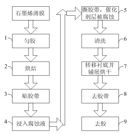
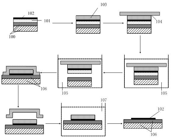
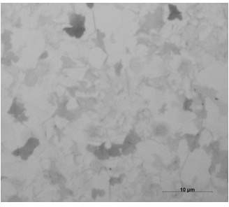
[0049] figure 2 It is a structural schematic diagram of the substrate transfer process of the graphene film in Example 1 of the present invention. Such as figure 2 As shown, first, a photoresist 9912 is spin-coated on the surface of a graphene film 102 prepared by CVD using nickel 101 as a catalyst, such as image 3 Shown is an optical photo of a graphene film attached to a nickel substrate, spin-coated at 4000 rpm for 1 minute, baked at 115°C for 2 minutes to harden the film; then attach a layer of thermal release tape on the surface of the colloid 103 104, heat release tape is required to completely cover the surface of the organic colloid; then soak it in 0.5mol / L ferric chloride aqueous solution 105, in the solution, hold the corner of the tape with tweezers and gently tear it, the tape will connect the colloid, The gr...
Embodiment 2
[0050] Example 2: Transfer of a thin film of graphene on metallic nickel to a plastic substrate.
[0051] The specific steps are similar to those in Example 1, but the target substrate used is a plastic substrate, and the graphene film can also be successfully transferred to the plastic substrate.
Embodiment 3
[0052] Example 3: Transfer of a graphene film on metallic copper to a silicon dioxide / silicon substrate.
[0053] The specific steps are similar to Example 1, but the metal catalyst layer of CVD growth graphene is copper, and the etching solution is ferric nitrate solution, and the graphene film can also be successfully transferred to the silicon dioxide / silicon substrate.
PUM
 Abstract
Description
Claims
Application Information