Self-assembly preparation method for floating gate layer of silicon nitride dielectric film with embedded metal tungsten quantum dots

A technology of tungsten quantum and silicon nitride, which is applied in the field of self-assembly to prepare the floating gate layer of silicon nitride dielectric film embedded with metal tungsten quantum dots, which can solve the constraints of miniaturization, quantum dot density and size distribution, and the uneven electrical performance of memory cells etc. to achieve the effects of small size, anti-oxidation and high density

Inactive Publication Date: 2012-07-18
SUN YAT SEN UNIV
View PDF1 Cites 0 Cited by
  • Summary
  • Abstract
  • Description
  • Claims
  • Application Information

AI Technical Summary

Problems solved by technology

With the miniaturization of quantum dot non-volatile memory, the inhomogeneity of the electrical properties of memory cells brought about by the inhomogeneity of quantum dot density and size distribution is the key problem restricting its miniaturization.

Method used


Image

  • Self-assembly preparation method for floating gate layer of silicon nitride dielectric film with embedded metal tungsten quantum dots
  • Self-assembly preparation method for floating gate layer of silicon nitride dielectric film with embedded metal tungsten quantum dots
  • Self-assembly preparation method for floating gate layer of silicon nitride dielectric film with embedded metal tungsten quantum dots

Examples


Embodiment 1

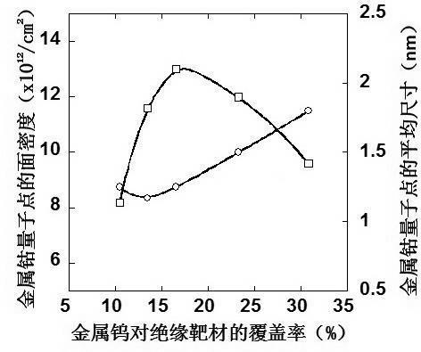
[0025] The target for magnetron sputtering is a 2-inch silicon nitride target, on which 5mmx5mmx1.5mm small metal tungsten pieces are evenly placed, and the coverage of the metal tungsten small pieces on the silicon nitride target is adjusted, and the range is 10%~ 30%. After standard cleaning of P-type (100) silicon wafers, silicon dioxide is grown by thermal oxidation with a thickness of about 5nm. Put the above-mentioned silicon wafer into the magnetron sputtering reaction chamber. The sputtering conditions are: the vacuum degree of the chamber body is 4x10 -6 Pa, the argon flow rate is 8sccm, the RF power applied to the target is 100W, the working pressure is 0.08Pa, the substrate is not heated, the substrate speed is 75rpm / min, and the sputtering film thickness is 5nm. The thin film embedded with metal tungsten quantum dots was vacuum annealed in situ in the sputtering chamber at a temperature of 800 degrees for 1 hour. figure 1 The graph showing the relationship betwe...


PUM


Abstract

The invention discloses a self-assembly preparation method for a floating gate layer of a silicon nitride dielectric film with embedded metal tungsten quantum dots. According to the invention, at a room temperature, a magnetron sputtering method is adopted to prepare the silicon nitride dielectric film with the embedded metal tungsten quantum dots, and the film serves as a floating gate structure of a non-volatile memory; a sputtering target material is formed by small metal tungsten blocks on a silicon nitride target material, and the nano-scale metal tungsten quantum dots, which are uniformly distributed on the silicon nitride dielectric film, can be obtained through cosputtering at the room temperature; and the size and density of the metal tungsten quantum dots can be adjusted through adjusting the amount of the small metal blocks, namely by adjusting the coverage rate of the small metal blocks to the silicon nitride target material. The high-density metal tungsten quantum dots prepared by the invention have favorable thermal stability at the high temperature of 800 DEG C and are easy to compatible with a CMOS (Complementary Metal Oxide Semiconductor) technology. The silicon nitride dielectric film with embedded high-density metal tungsten quantum dots serves as the floating gate layer of the non-volatile memory and has good charge storage characteristics.

Description

[0001] technical field [0002] The invention relates to a self-assembly method for preparing a floating gate layer of a silicon nitride dielectric film embedded with metal tungsten quantum dots. [0003] Background technique [0004] In recent years, the Flash memory market has been expanding day by day, and higher requirements have been put forward for its integration and performance. According to ITRS 2010, the Technology node of Flash memory will enter the order of 20nm or below in the near future. However, the miniaturization of traditional flash memory with polysilicon floating gate structure is facing severe challenges. First of all, the miniaturization of flash memory greatly reduces the reliability of data storage and shortens the charge accumulation time. In addition, miniaturization aggravates the short-channel effect, increasing power consumption and interference between memory units. In order to solve these problems, a breakthrough must be made in the struct...

Claims


Application Information

Patent Timeline
IPC IPC(8): H01L21/285
Inventor 裴艳丽王钢
Owner SUN YAT SEN UNIV
Why Eureka
Try Eureka