Preparation method for back-contact crystalline silicon solar cell based on plasma etching technology

A back-contact, solar cell technology, applied in the field of solar cells, can solve the problems of large investment in the industrialization of lithography opening, influence of reliability and stability, and low opening accuracy, so as to facilitate industrial production and high conversion efficiency. , to ensure the effect of passivation performance

Inactive Publication Date: 2012-07-18
SUN YAT SEN UNIV
View PDF5 Cites 9 Cited by
  • Summary
  • Abstract
  • Description
  • Claims
  • Application Information

AI Technical Summary

Problems solved by technology

The industrialization of photolithography opening requires a lot of investment, and laser opening is likely to cause a lot of thermal damage and form a large recombination center. At the same time, the reliability and stability of the laser directly affect the quality of battery products, while screen printing corrosive paste opening low precision

Method used


Image

  • Preparation method for back-contact crystalline silicon solar cell based on plasma etching technology
  • Preparation method for back-contact crystalline silicon solar cell based on plasma etching technology
  • Preparation method for back-contact crystalline silicon solar cell based on plasma etching technology

Examples


Embodiment 1

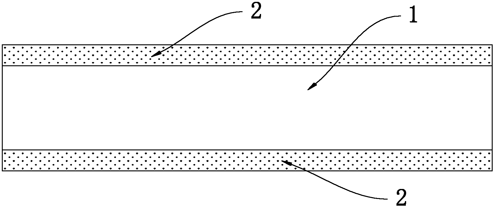
[0046] Step 1: Put the silicon wafer substrate 1 into a high-temperature diffusion furnace, 3 As a phosphorus source, an n-type layer 2 is formed on both sides of the silicon wafer through high-temperature diffusion doping with phosphorus, and the sheet resistance of the n-type layer 2 is 40-50Ω / □.

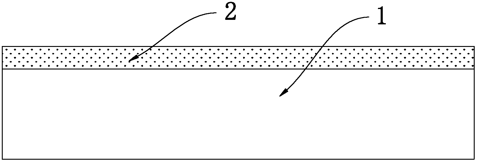
[0047] Step 2: Using HF / HNO 3 The mixed solution removes the n-type layer 2 on the back side of the silicon wafer substrate 1 through a single-side etching device, wherein the concentration of the HF solution is 49%, and the HNO 3 Solution concentration is 69%, HF solution and HNO 3 The solution volume ratio is 1:3;

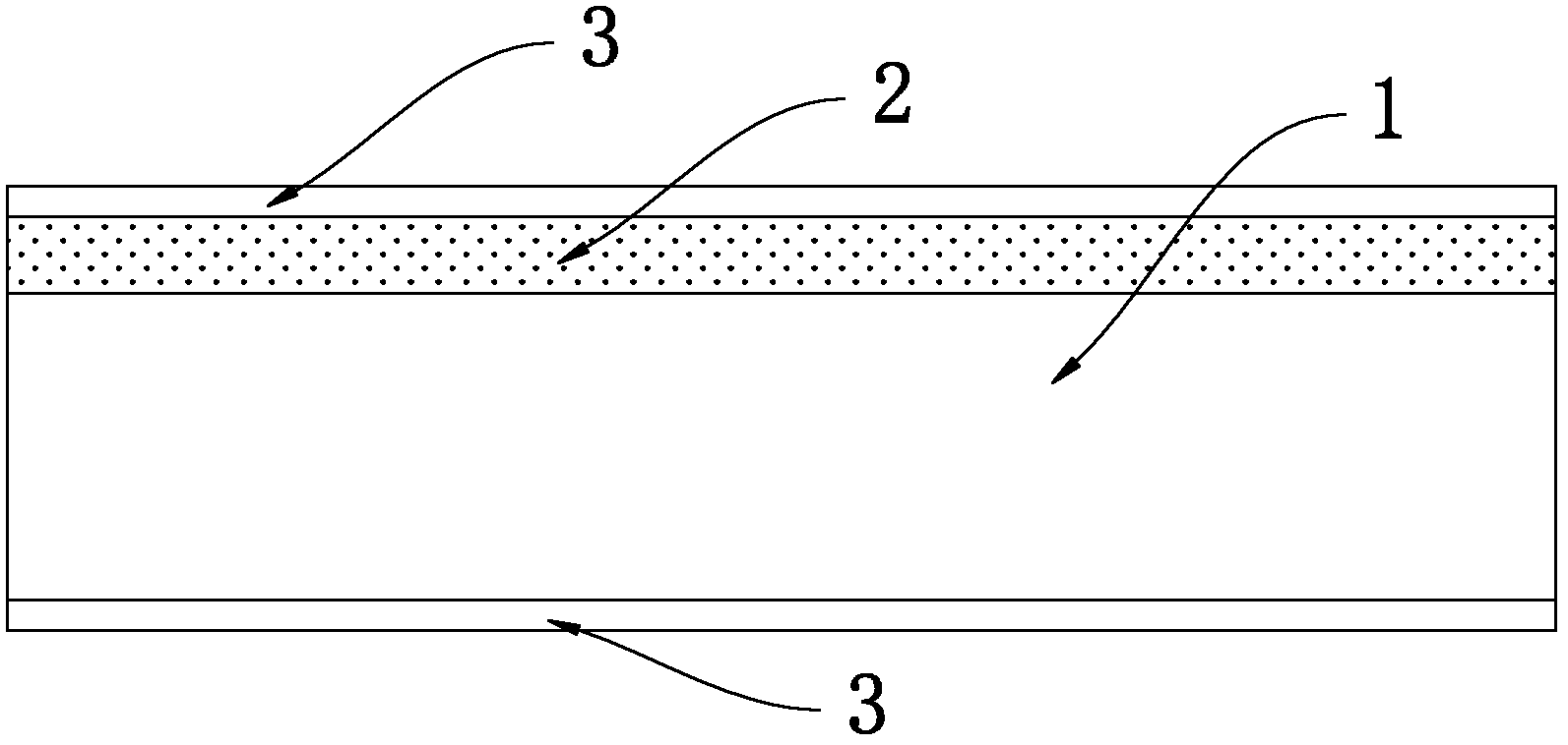
[0048] Step 3: Put the silicon wafer substrate 1 into an oxidation furnace, and dry thermal oxidation on both sides of the silicon wafer substrate 1 at high temperature to form a thermal oxidation layer 3, the thermal oxidation layer 3 is a silicon dioxide layer, and The thickness is 5-15nm.

[0049] Step 4: Coating a layer of silicon nitride (SiNx:H) on the back...

Embodiment 2

[0058] Step 1: Put the silicon wafer substrate 1 into a high-temperature diffusion furnace, 3 As a phosphorus source, an n-type layer 2 is formed on both sides of the silicon wafer through high-temperature diffusion doping with phosphorus, and the sheet resistance of the n-type layer 2 is 50-60Ω / □.

[0059] Step 2: using KOH solution to remove the n-type layer 2 on the back side of the silicon wafer substrate 1 through single-side etching equipment, wherein the concentration of the KOH solution is 20%;

[0060] Step 3: Put the silicon wafer substrate 1 into an oxidation furnace, and form a thermal oxidation layer 3 by dry thermal oxidation on both sides of the silicon wafer substrate 1 at high temperature. The thermal oxidation layer 3 is a silicon dioxide layer with a thickness of 35~50nm.

[0061] Step 4: Coating a layer of silicon nitride (SiNx:H) on the back of the silicon wafer substrate 1 by PECVD equipment to form a back silicon nitride layer 4, and the back silicon ni...

Embodiment 3

[0070] Step 1: Put the silicon wafer substrate 1 into a high-temperature diffusion furnace, 3 As a phosphorus source, the n-type layer 2 is formed on both sides of the silicon wafer through high-temperature diffusion and doping of phosphorus, and the sheet resistance of the n-type layer 2 is 60-70Ω / □.

[0071] Step 2: using NaOH solution to remove the n-type layer 2 on the back side of the silicon wafer substrate 1 through single-side etching equipment, wherein the concentration of the KOH solution is 20%;

[0072] Step 3: put the silicon wafer substrate into an oxidation furnace, dry thermal oxidation on both sides of the silicon wafer substrate 1 at high temperature to form a thermal oxide layer 3 with a thickness of 15-30 nm.

[0073] Step 4: Coating a layer of silicon nitride (SiNx:H) on the back of the silicon wafer substrate 1 by PECVD equipment to form a back silicon nitride layer 4, and the back silicon nitride layer 4 and the silicon dioxide layer form a silicon dioxi...


PUM

PropertyMeasurementUnit
thicknessaaaaaaaaaa
thicknessaaaaaaaaaa
thicknessaaaaaaaaaa

Abstract

The invention discloses a preparation method for a back-contact crystalline silicon solar cell based on plasma etching technology, which comprises the steps of forming a silicon dioxide layer and a silicon nitride layer on a silicon wafer substrate by heat oxidation, thereby forming a double-layer passivating composite membrane; on a back screen mesh of the silicon wafer substrate, printing an aluminum slurry layer which is providing with hollow array patterns and no frit and sintering; placing a silicon wafer to a plasma etching device, and removing silicon nitride on the hollow patterns on the back surface of the silicon wafer substrate by plasmas; printing an aluminum slurry layer with frit on a back screen mesh of the silicon wafer; and sintering and burning through the thin silicon dioxide layer on the back surface by drying so as to form a point contact electrode, or a line contact electrode on the back surface and a local aluminum back-surface-field. The method adopts the mature technology of screen mesh printing, plasma etching and the like, the preparation of high-efficiency back-contact cell is completed, the investment cost is low, the market prospect is wide; and the cell can be produced in an industrialization way.

Description

technical field [0001] The invention belongs to the technical field of solar cells, and in particular relates to a method for preparing a rear contact crystalline silicon solar cell based on plasma etching technology. Background technique [0002] With the continuous reduction of solar cell production costs and the continuous improvement of solar cell efficiency, the photovoltaic industry has developed rapidly under the policy support of governments of various countries, and has become a leader in the new energy industry in recent years. In order to achieve lower production costs and higher conversion efficiency, researchers from various departments and units have proposed different new processes, new methods, and new structures. The traditional aluminum back field process cannot meet the requirements of low recombination rate on the back of thin silicon wafers. The back contact cell is considered to be a method that can reduce the metal-semiconductor contact area, passivate...

Claims


Application Information

Patent Timeline
Patent Type & Authority Applications(China)
IPC IPC(8): H01L31/18
CPCY02P70/50
Inventor 沈辉刘家敬邹禧武陈达明
Owner SUN YAT SEN UNIV
Why Eureka
Try Eureka