High-drive-current III-V metal oxide semiconductor device

An oxide semiconductor, III-V technology, used in semiconductor devices, electrical components, circuits, etc., can solve the problem of low conduction band state density, limiting device drive current, MOS interface state density, and channel carrier mobility. and other problems, to achieve the effect of low interface state density, increase driving current, and reduce scattering

Inactive Publication Date: 2012-07-25
INST OF MICROELECTRONICS CHINESE ACAD OF SCI
View PDF3 Cites 21 Cited by
  • Summary
  • Abstract
  • Description
  • Claims
  • Application Information

AI Technical Summary

Problems solved by technology

However, the properties of this interface still cannot be compared with SiO 2 Compared with Si, the high-k gate dielectric material is directly grown on the surface of the high-mobility channel, and the high density of the MOS interface state will le...

Method used


Image

  • High-drive-current III-V metal oxide semiconductor device
  • High-drive-current III-V metal oxide semiconductor device
  • High-drive-current III-V metal oxide semiconductor device

Examples


Embodiment Construction

[0023] In order to make the object, technical solution and advantages of the present invention clearer, the present invention will be described in further detail below in conjunction with specific embodiments and with reference to the accompanying drawings.

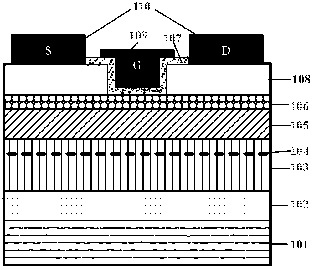
[0024] Such as figure 1 as shown, figure 1 It is a structural diagram of a III-V group MOS device with a high driving current provided by the present invention, and the device includes: a single crystal substrate 101; a buffer layer 102 formed on the upper surface of the single crystal substrate 101; A quantum well bottom barrier layer 103 formed on the upper surface of the layer 102; a planar doped layer 104 formed in the quantum well bottom barrier layer 103; a high mobility layer formed on the quantum well bottom barrier layer 103 upper surface Quantum well channel 105; an interface control layer 106 formed on the upper surface of the high-mobility quantum well channel 105; a high-K gate dielectric 107 and raised sour...


PUM


Abstract

The invention discloses a high-drive-current III-V metal oxide semiconductor device which comprises a single crystal substrate, a buffer layer, a quantum-well bottom barrier layer, a planar doped layer, a high-mobility quantum-well channel, an interface control layer, a high K gate dielectric, an elevated source/drain layer, a metal gate structure and a source/drain contact metal layer, wherein the buffer layer is formed on the upper surface of the single crystal substrate; the quantum-well bottom barrier layer is formed on the upper surface of the buffer layer; the planar doped layer is formed in the quantum-well bottom barrier layer; the high-mobility quantum-well channel is formed on the upper surface of the quantum-well bottom barrier layer; the interface control layer is formed on the upper surface of the high-mobility quantum-well channel; the high K gate dielectric and the elevated source/drain layer are formed on the upper surface of the interface control layer; the metal gate structure is formed on the high K gate dielectric; and the source/drain contact metal layer is formed on the elevated source/drain layer. According to the invention, a dangling bond on an MOS (metal oxide semiconductor) interface is passivated by using an interface control layer technology, thereby realizing the low interface state density, reducing the scattering of current carriers in the channel, improving the concentration of two-dimensional electron gas or two-dimensional hole gas in a channel layer, and satisfying the requirements of a high-performance III-V CMOS (complementary metal oxide semiconductor) technology.

Description

technical field [0001] The invention relates to the technical field of semiconductor integrated circuit manufacturing, in particular to a III-V group metal oxide semiconductor (MOS) device with a high driving current realized by adopting interface control layer, bottom barrier plane doping and raising source and drain, Applied to high-performance III-V MOS devices. Background technique [0002] When the complementary metal-oxide-semiconductor (CMOS) technology enters the 22nm technology node, it is difficult to improve device performance by scaling down. The use of new materials and new devices has become an important research direction to continue to improve the performance of CMOS devices. III-V semiconductor materials have become a hot topic in current research because of their high electron mobility. However, high-quality thermally stable gate dielectric materials have been the main obstacle for the application of III-V semiconductors in large-scale CMOS integrated circ...

Claims


Application Information

Patent Timeline
IPC IPC(8): H01L29/778H01L29/06
Inventor 刘洪刚常虎东卢力薛百清王虹孙兵
Owner INST OF MICROELECTRONICS CHINESE ACAD OF SCI
Why Eureka
Try Eureka