Method for producing amorphous indium gallium zinc oxide thin film by atomic layer deposition

A technology of indium gallium zinc oxide and atomic layer deposition, which is applied in coating, gaseous chemical plating, metal material coating process, etc., can solve the problem that it is difficult to obtain a large-area surface film with uniform thickness and uniform electrical performance of the device To avoid adverse effects on performance, device performance and reliability, etc., to achieve optimized electrical properties, less defects such as oxygen vacancies, and low deposition temperature

Inactive Publication Date: 2012-08-01
FUDAN UNIV
View PDF3 Cites 19 Cited by
  • Summary
  • Abstract
  • Description
  • Claims
  • Application Information

AI Technical Summary

Problems solved by technology

However, the quality of IGZO films deposited by these methods is poor, usually containing some oxygen vacancies, and requires some post-processing, such as thermal annealing, etc.
These post-annealing treatments are usually performed at relatively high temperatures, thus limiting its application in the field of devices based on flexible substrates and glass substrates
In addition, high temperature annealing will also have a certain negative impact on the performance and reliability of the device
On the other hand, it is difficult to obtain a thin film with uniform surface thickness and atomic composition over a large area using the above method, which will adversely affect the uniformity of the electrical properties of the entire device.

Method used


Image

  • Method for producing amorphous indium gallium zinc oxide thin film by atomic layer deposition
  • Method for producing amorphous indium gallium zinc oxide thin film by atomic layer deposition
  • Method for producing amorphous indium gallium zinc oxide thin film by atomic layer deposition

Examples


Embodiment Construction

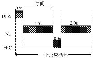
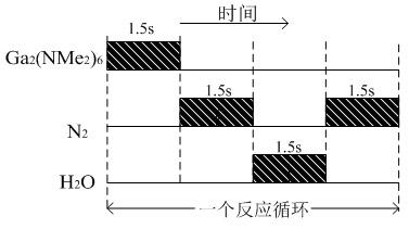
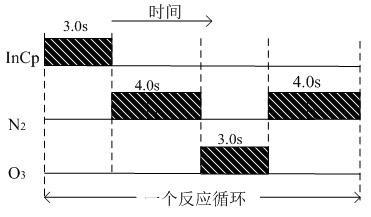
[0029] The invention will be described in detail below in conjunction with the accompanying drawings and specific examples. covered with Al 2 o 3 On the monocrystalline silicon substrate of the dielectric film, the IGZO film is grown by atomic layer deposition, and the ratio of the reaction cycles of each oxide is In 2 o 3 : Ga 2 o 3 :ZnO=1:1:1.

[0030] Step 1, atomic layer deposition growth of ZnO. Using ALD technology to deposit ZnO to grow a reaction cycle, such as figure 1 , where the shaded part indicates that the gas is introduced into the reaction chamber. The reaction source for depositing ZnO is diethyl zinc, the oxidant is water, and the temperature of the reaction chamber is controlled at 100-300°C during the growth process. o C range.

[0031] The specific process of depositing ZnO by ALD technology includes the following steps: (1) Diethyl zinc vapor is passed into the ALD reaction chamber, and the pulse time of the diethyl zinc vapor is 0.5 s. (2) Inj...


PUM


Abstract

The invention belongs to the technical field of semiconductor integrated circuits, and particularly discloses a method for growing an amorphous indium gallium zinc oxide thin film by the ALD (atomic layer deposition) technique. The method mainly includes the steps: using diethylzinc as a reaction source for growing ZnO, and using water or hydrogen peroxide as oxidant; using Ga2 (NMe2)6 as a reaction source for growing Ga2O3, and using water as oxidant; growing In2O3 for multiple cycles, using cyclopentadienylindium as a reaction source for growing In2O3, and using mixture of water and oxygen or ozone as oxidant; and repeating the steps for multiple times as required to obtain an IGZO thin film of certain thickness. The temperature of a reaction chamber in growth is controlled within a range of from 100 DEG C to 300 DEG C. In addition, the steps above are free to order and combine. The IGZO thin film grown by the method is high in uniformity, density and shape retention, suitable for large-area disposition, and widely applicable to the fields of thin film transistors, thin film transistor memories and transparent electronic devices.

Description

technical field [0001] The invention belongs to the technical field of semiconductor integrated circuits, and specifically relates to a method for growing IGZO (amorphous indium gallium zinc oxide) thin films by atomic layer deposition (ALD) for thin film transistors (TFTs), TFT tube memories and transparent electronic devices. method. Background technique [0002] In recent years, due to intensified competition, the display market has shown a trend of accelerated growth. As an important component of the display, TFT has received more and more attention and research, especially the TFT device using amorphous oxide semiconductor as the conductive channel has become a research hotspot at home and abroad. Compared with polysilicon or organic thin-film transistors, transistors using amorphous oxide semiconductors as conductive channels have outstanding advantages such as high carrier mobility, high optical transparency, and more stable threshold voltage. As a transparent oxide...

Claims


Application Information

Patent Timeline
Patent Type & Authority Applications(China)
IPC IPC(8): C23C16/40C23C16/44H01L21/205
Inventor 丁士进崔兴美陈笋
Owner FUDAN UNIV
Why Eureka
Try Eureka