Method for preparing one-dimensional ZnO/SnO2 core/shell structure nano heterojunction semiconductor material

A technology of core-shell structure and nanomaterials, applied in nanotechnology, nanotechnology, metal material coating technology, etc., can solve the problems of complex process and toxicity, and achieve high repeatability, good crystallinity and strong controllability Effect

Active Publication Date: 2012-08-01
TECHNICAL INST OF PHYSICS & CHEMISTRY - CHINESE ACAD OF SCI
View PDF2 Cites 21 Cited by
  • Summary
  • Abstract
  • Description
  • Claims
  • Application Information

AI Technical Summary

Problems solved by technology

Among them, Qin Kuang et al. (Qin Kuang, Zhiyuan Jiang, Zhaoxiong Xie, Shuichao Lin, Zhiwei Lin, Suyuan Xie, Rongbin Huang, and Lansun Zheng, J. Am. Chem. Soc. 2005,127, 11777-11784) adopted Preparation of ZnO/SnO 2 The method of core-shell nanostructure requires the use of highly toxic gas SnH 4 It is risky to realize the coating of ZnO as a

Method used


Image

  • Method for preparing one-dimensional ZnO/SnO2 core/shell structure nano heterojunction semiconductor material
  • Method for preparing one-dimensional ZnO/SnO2 core/shell structure nano heterojunction semiconductor material
  • Method for preparing one-dimensional ZnO/SnO2 core/shell structure nano heterojunction semiconductor material

Examples


Embodiment 1

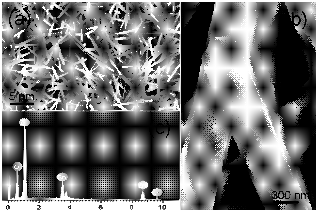
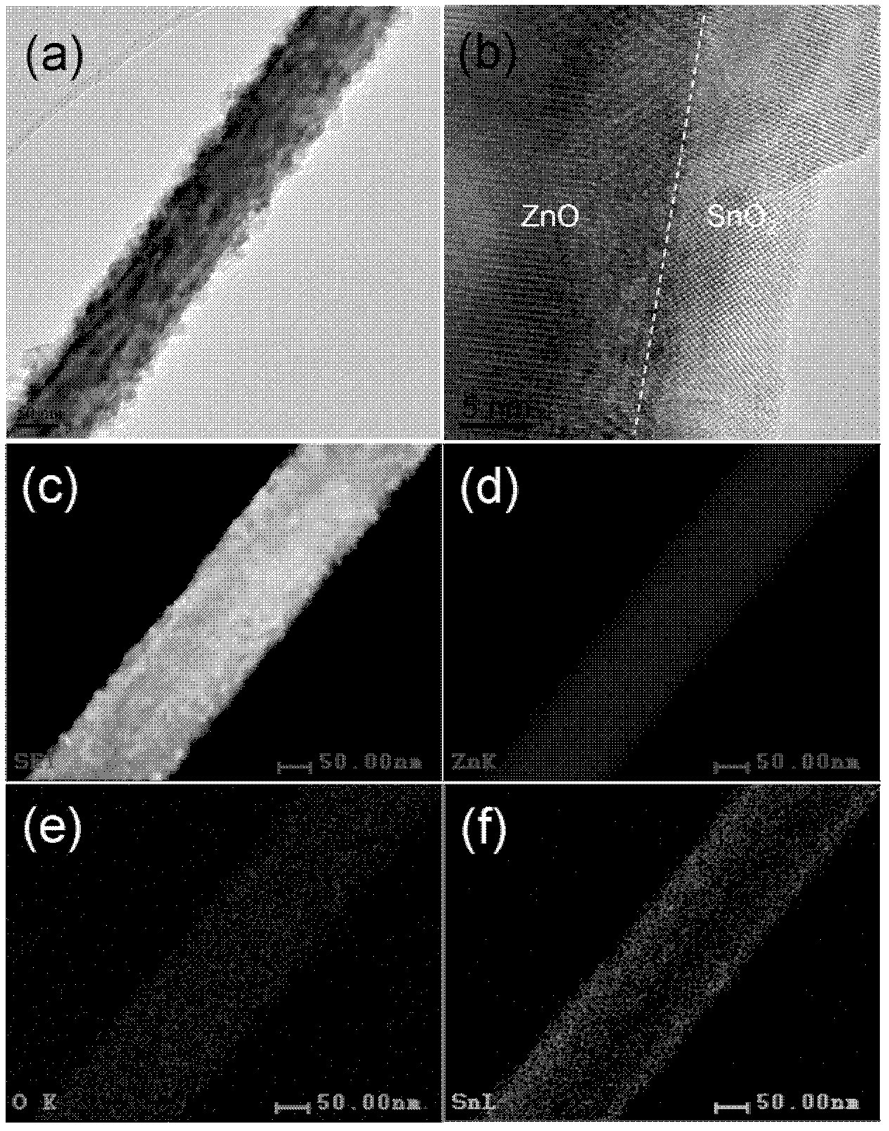
[0027] Take 2g of Zn powder and put it into the ceramic boat, then place the silicon chip substrate on the Zn powder, then place the ceramic boat in the high temperature heating zone of the tube furnace; turn on the mechanical pump, and when the pressure in the furnace drops to 0.1Pa, Introduce 20 sccm of air, control the pressure in the furnace to 80 Pa; raise the high temperature zone of the tube furnace to 550°C, the heating rate is 20°C / min, and the reaction time is 1 hour; after the reaction is completed, wait for the tube furnace to cool down to room temperature After that, take out the silicon wafer, which is loaded with ZnO nanorods;

[0028] Take 3g of SnO powder and put it into a ceramic boat, and then place it in the high-temperature heating zone of the tube furnace; place the silicon chip loaded with ZnO nanorods in the low-temperature deposition zone of the tube furnace; turn on the mechanical pump, and wait until the pressure in the furnace When it is reduced to ...

Embodiment 2

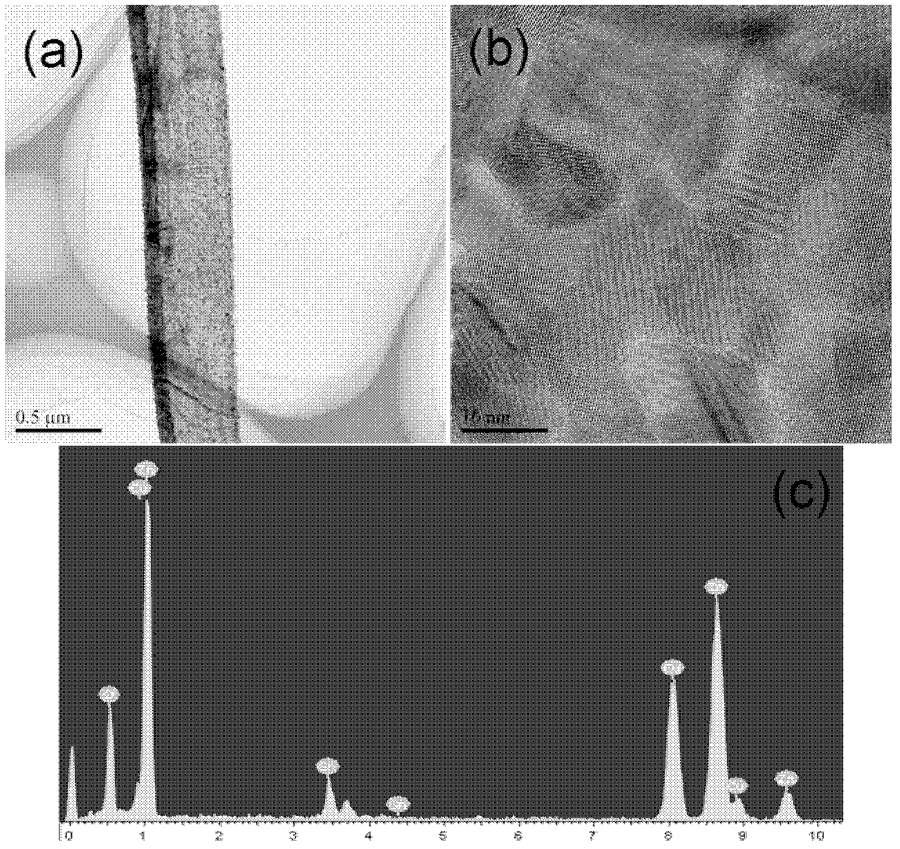
[0030] Get 2g of Zn powder and put it into the ceramic boat, then place the ceramic chip substrate on the Zn powder, then place the ceramic boat in the high temperature heating zone of the tube furnace; turn on the mechanical pump, and when the pressure in the furnace drops to 0.1Pa, Introduce 10 sccm of air, control the pressure in the furnace to 50 Pa; raise the high temperature zone of the tube furnace to 500°C, the heating rate is 15°C / min, and the reaction time is 2 hours; after the reaction is completed, wait for the tube furnace to cool down to room temperature Finally, take out the ceramic sheet, which is loaded with ZnO nanorods;

[0031] Take 3g of SnO powder and put it into a ceramic boat, and then place it in the high-temperature heating zone of the tube furnace; place the ceramic sheet loaded with ZnO nanorods in the low-temperature deposition zone of the tube furnace; turn on the mechanical pump and wait until the pressure in the furnace When it is reduced to 0.1...

Embodiment 3

[0033] Take 2g of Zn powder and put it into the ceramic boat, then put the quartz sheet substrate on the Zn powder, then place the ceramic boat in the high temperature heating zone of the tube furnace; turn on the mechanical pump, and when the pressure in the furnace drops to 0.1Pa, Introduce 30 sccm of air, control the pressure in the furnace to 150 Pa; raise the high temperature zone of the tube furnace to 600°C, the heating rate is 25°C / min, and the reaction time is 0.5 hours; after the reaction is completed, wait for the tube furnace to cool down to room temperature Finally, take out the quartz sheet, which is loaded with ZnO nanorods and a small amount of nanobelts;

[0034] Take 3g of SnO powder and put it into a ceramic boat, and then place it in the high-temperature heating zone of the tube furnace; place the quartz sheet loaded with ZnO nanorods in the low-temperature deposition zone of the tube furnace; turn on the mechanical pump and wait until the pressure in the fu...


PUM


Abstract

The invention discloses a method for preparing a one-dimensional ZnO/SnO2 core/shell structure nano heterojunction semiconductor material. According to the method, a one-dimensional ZnO nanomaterial is coated with SnO2 through thermal evaporation to form the one-dimensional ZnO/SnO2 core/shell structure nano heterojunction semiconductor material. The method is high in repeatability and controllability, and environment-friendly, and the SnO2 is coated uniformly. The prepared one-dimensional ZnO/SnO2 core/shell structure nano heterojunction semiconductor material has high research value and wide application prospect in the fields of solar cells, gas sensors, photocatalysis and the like.

Description

technical field [0001] The invention relates to a one-dimensional ZnO / SnO 2 A method for preparing a nano-heterojunction semiconductor material with a core-shell structure. It belongs to the field of nanometer semiconductor technology. Background technique [0002] At room temperature, ZnO and SnO 2 The bandgap widths are 3.37 and 3.6 eV, respectively. As an important wide bandgap semiconductor oxide, ZnO can be used in many fields, such as solar cells, sensors, lasers, photocatalysis, etc. In addition, another important wide bandgap semiconductor oxide—SnO 2 , It also has a wide range of application values ​​in gas sensors, solar cells, transparent conductive electrodes, catalytic carriers, etc. In recent years, researchers have found that by combining ZnO and SnO 2 These two materials are combined to form ZnO / SnO 2 Compared with a single material, the composite material of the two has significantly improved in gas sensitivity, photocatalysis and nano-optoelectronic ...

Claims


Application Information

Patent Timeline
IPC IPC(8): C23C16/448C23C16/40C04B35/628B82Y30/00B82Y40/00
Inventor 孟祥敏黄兴
Owner TECHNICAL INST OF PHYSICS & CHEMISTRY - CHINESE ACAD OF SCI
Why Eureka
Try Eureka