Bulk-silicon-based manufacturing method for vertically stacked under-gate type silicon nano-wire metal oxide semiconductor field effect transistor (SiNWFET)

A vertical stacking, gate-behind technology, used in semiconductor/solid-state device manufacturing, semiconductor devices, electrical components, etc., can solve the problems of large interface state, unsuitable gate oxide layer of field effect transistors, inconvenience, etc., and achieve device current driving capability The effect of increasing the number of nanowires and simplifying the process flow

Inactive Publication Date: 2012-08-01
SHANGHAI HUALI MICROELECTRONICS CORP
View PDF5 Cites 13 Cited by
  • Summary
  • Abstract
  • Description
  • Claims
  • Application Information

AI Technical Summary

Problems solved by technology

This method can realize the vertically stacked silicon nanowire field effect transistor structure, but there is a disadvantage: when the SiGe layer is oxidized, Ge will be concentrated on the surface of the Si layer. SiGe alloy
Because GeO2 is soluble in water, it makes the subsequent process face great inconvenience. In addition, the dielectric constant of GeO2 is smaller than that of SiO2, and the interface state between GeO2 and Si is larger, so it is not suitable as the gate oxide layer of field effect transistor (FET).

Method used


Image

  • Bulk-silicon-based manufacturing method for vertically stacked under-gate type silicon nano-wire metal oxide semiconductor field effect transistor (SiNWFET)
  • Bulk-silicon-based manufacturing method for vertically stacked under-gate type silicon nano-wire metal oxide semiconductor field effect transistor (SiNWFET)
  • Bulk-silicon-based manufacturing method for vertically stacked under-gate type silicon nano-wire metal oxide semiconductor field effect transistor (SiNWFET)

Examples


Embodiment Construction

[0067] In order to make the above objects, features and advantages of the present invention more comprehensible, specific implementations of the present invention will be described in detail below in conjunction with the accompanying drawings.

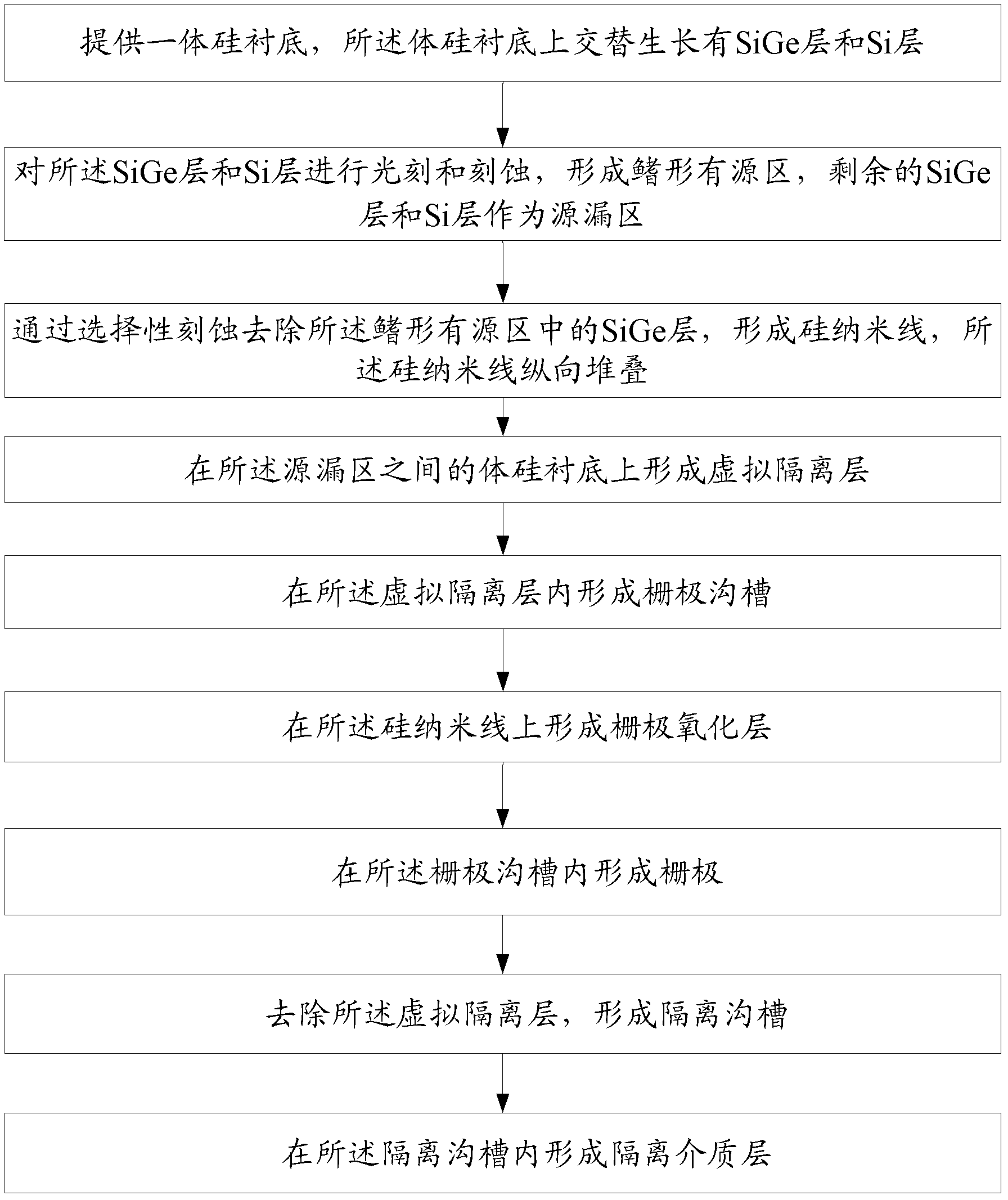
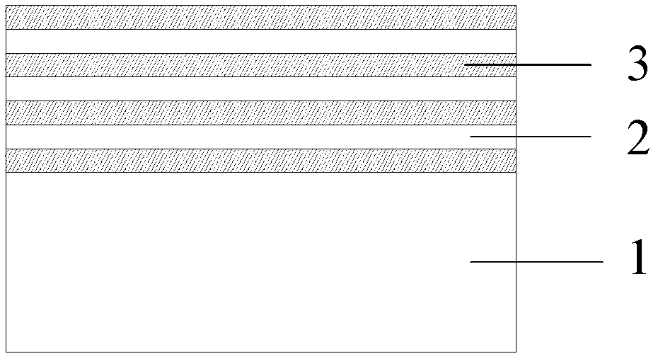
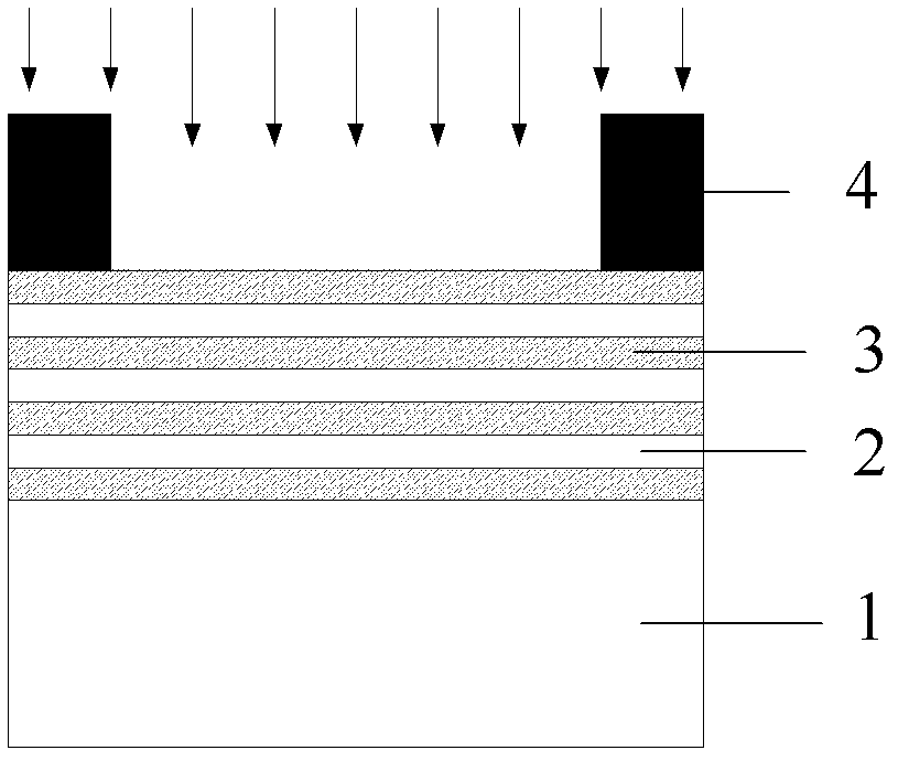
[0068] First, if Figure 19 As shown, in order to describe this embodiment more clearly, the length direction of the fin-shaped active region 5 or the subsequently formed silicon nanowire 6 is defined as the XX' direction, and the XX' direction runs through the gate 10 and the source and drain regions 17. The direction perpendicular to X-X' is Y-Y'. Combine below Figure 1 to Figure 19 A method for fabricating a bulk silicon-based vertical stacked gate-last SiNWFET according to an embodiment of the present invention will be described in detail.

[0069] Such as figure 1 As shown, the method for fabricating a bulk silicon-based vertically stacked gate-back SiNWFET according to an embodiment of the present invention includes the follo...


PUM

PropertyMeasurementUnit
diameteraaaaaaaaaa

Abstract

The invention discloses a bulk-silicon-based manufacturing method for a vertically stacked under-gate type silicon nano-wire metal oxide semiconductor field effect transistor (SiNWFET). The method comprises the following steps of: providing a bulk silicon substrate on which SiGe layers and Si layers are alternately grown; photo-etching and etching the SiGe layers and the Si layers to form fin-shaped active regions, and taking the residual SiGe layers and the residual Si layers as source and drain regions; selectively etching and removing the SiGe layers in the fin-shaped active regions to form silicon nano-wires which are vertically stacked; forming a virtual isolation layer on the bulk silicon substrate between the source region and the drain region; forming a gate trench in the virtual isolation layer; forming gate oxide layers on the silicon nano-wires; forming a gate in the gate trench; removing the virtual isolation layer to form an isolated trench; and forming an isolation dielectric layer in the isolated trench. Due to the adoption of the virtual isolation layer, control over the contour of the gate trench is facilitated; the conventional gate oxide layers are adopted; and the silicon nano-wires are vertically stacked, so that the integration level and current driving capability of a device can be improved.

Description

technical field [0001] The invention relates to the field of semiconductor manufacturing, in particular to a bulk silicon-based vertically stacked gate-back type silicon nanowire field effect transistor (SiNWFET) preparation method. Background technique [0002] In the prior art, reducing the size of transistors to increase the working speed and integration of chips and reduce the power consumption density of chips has always been the goal pursued by the development of the microelectronics industry. In the past forty years, the development of microelectronics industry has been following Moore's Law. At present, the physical gate length of field effect transistors is close to 20nm, and the gate dielectric is only a few layers thick of oxygen atoms. It is difficult to improve the performance by reducing the size of traditional field effect transistors, mainly because of the short channel Channel effect and gate leakage current deteriorate the switching performance of the tran...

Claims


Application Information

Patent Timeline
Patent Type & Authority Applications(China)
IPC IPC(8): H01L21/762H01L21/28H01L21/02H01L21/336
Inventor 黄晓橹谢欣云
Owner SHANGHAI HUALI MICROELECTRONICS CORP
Why Eureka
Try Eureka