PVD (Physical Vapor Deposition) super-black coating
A black coating and coating technology, applied in coating, metal material coating process, ion implantation plating, etc., can solve the problems of low sputtering deposition energy, rough film layer, high evaporation rate of deposited ions, and achieve surface The effect of high finish, high film compactness and high film adhesion
- Summary
- Abstract
- Description
- Claims
- Application Information
AI Technical Summary
Problems solved by technology
Method used
Image
Examples
Embodiment 1
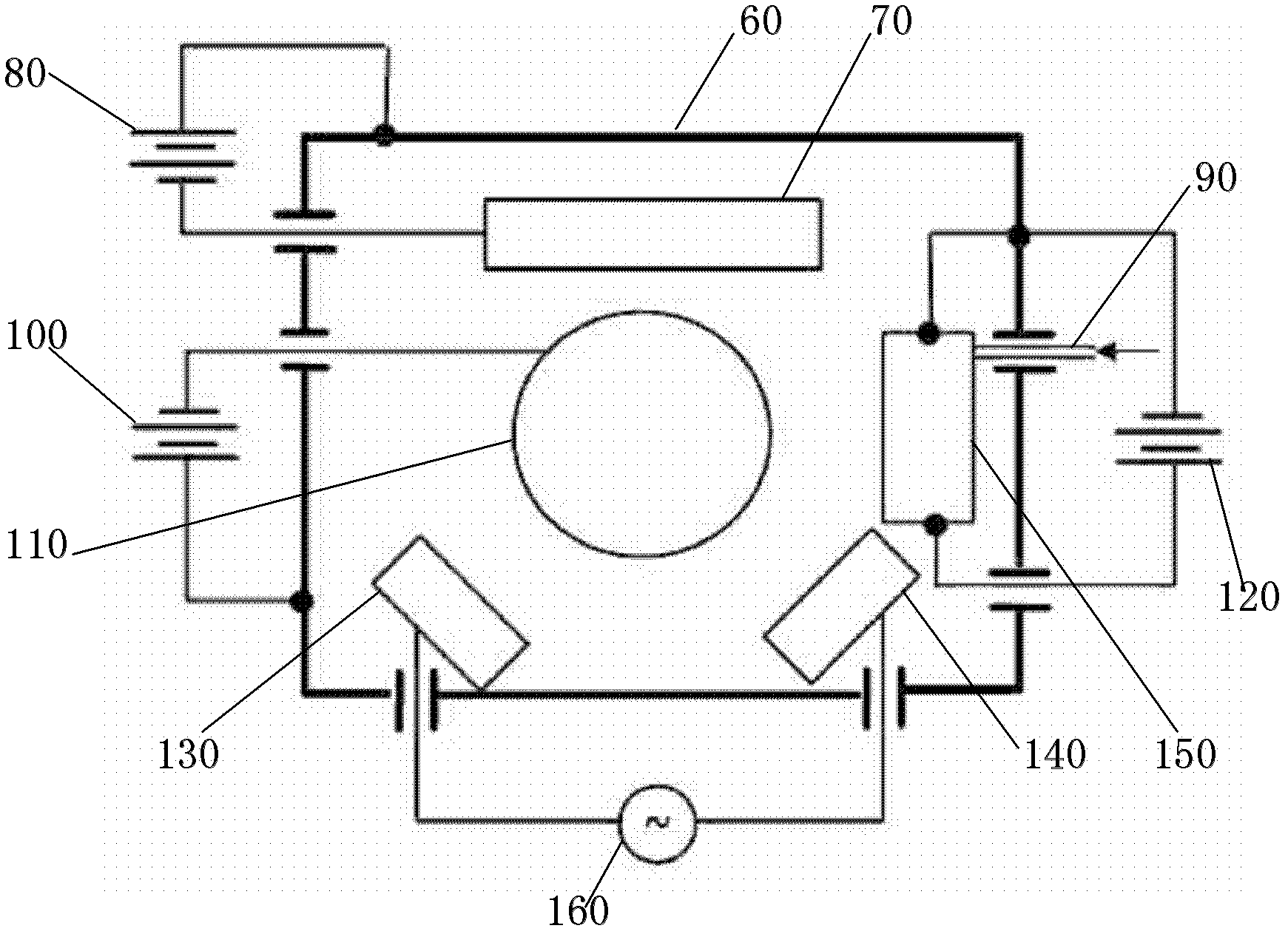
[0026] please see image 3 As shown, a multifunctional PVD coating machine in the embodiment of the present invention includes a vacuum chamber 60, a conductive workpiece turret 110 arranged in the vacuum chamber, a plasma arc evaporation source 70 and an arc power supply 80, and also includes a pulse bias power supply 100 , intermediate frequency sputtering source 130 and 140, intermediate frequency power supply 160, gas ion source 150, ion source power supply 90, described pulse bias power supply 100 and plasma arc evaporation source 70, intermediate frequency sputtering source 130 and 140, gas ion source 150 pass The four sets of switches are individually controlled, and the pulse bias power supply 100, the plasma arc evaporation source 70, the intermediate frequency sputtering sources 130 and 140, and the gas ion source 150 can all work independently or in coordination.
[0027] The conductive workpiece turret 110 is insulated from the vacuum chamber 60, and the vacuum cha...
Embodiment 2
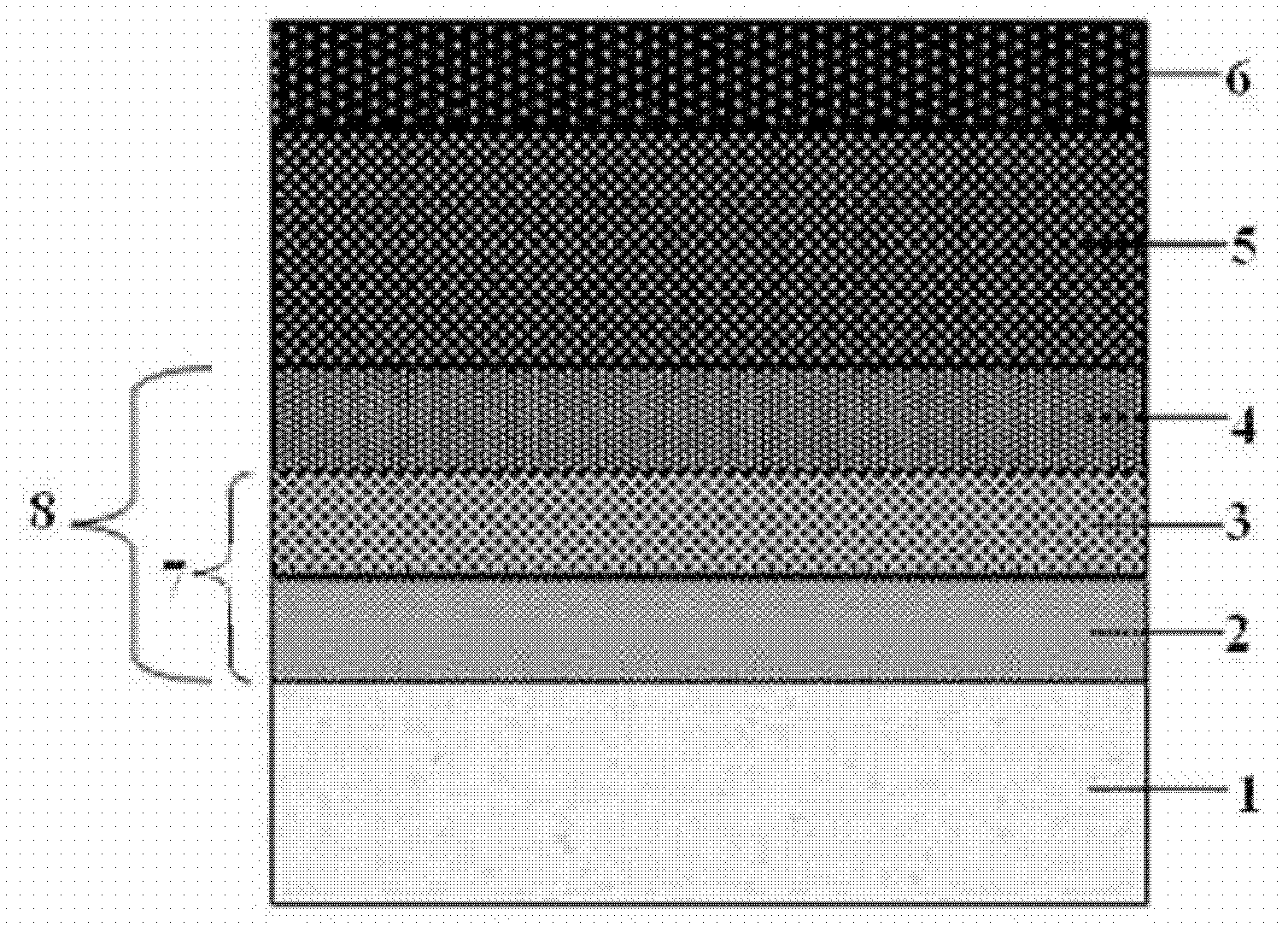
[0032] The substrate 1 is prepared, and the material of the substrate is conductive metal material. The film layer 2 is deposited using the multifunctional PVD coating machine described in the embodiment. The specific method is: using the plasma multi-arc deposition device 70 , using a low-voltage, high-current power source 80 to generate arc power on the surface of the target, generating a target plasma, and depositing the plasma on the substrate 1 . And by using the pulse bias power supply 100, a negative bias voltage of 300-600V is applied on the surface of the substrate 1, and the thickness of the metal film layer 2 is controlled at 0.05-0.15um.
[0033] Deposit the film layer 3, turn on the plasma multi-arc deposition device 70, use a low-voltage, high-current power supply 80 to generate arc power on the surface of the metal film layer 2, generate plasma, and deposit the plasma on the base metal film layer 2 while using an intermediate frequency The sputtering sources 13...
PUM
 Abstract
Description
Claims
Application Information


