

Cantilever type IC (Integrated Circuit) chip stack package of BT (Bismaleimide Triazine) substrate and production method of cantilever type IC chip stack package
A technology of chip stacking and BT substrates, which is applied in the field of electronic information automation components manufacturing, can solve the problems of increased line density and line length, difficult packaging, and increased short circuit of welding lines, so as to reduce the possibility, avoid short circuit of lines, and eliminate exposure The effect of the welding line
- Summary
- Abstract
- Description
- Claims
- Application Information
AI Technical Summary
Problems solved by technology
Method used
Image

Examples
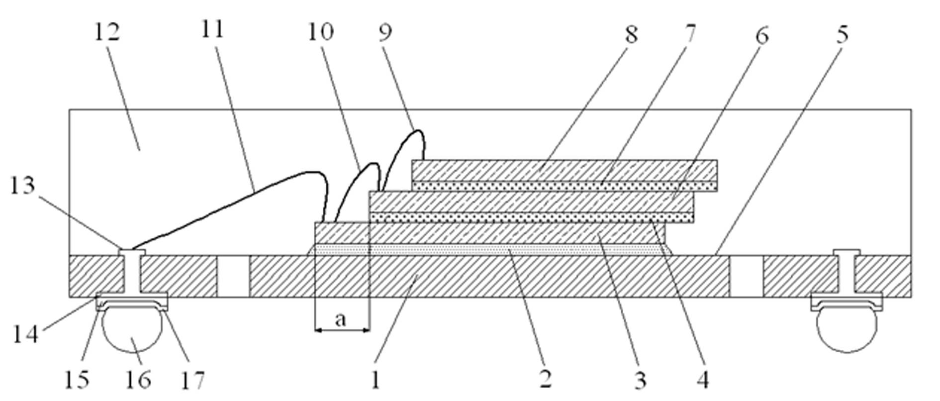
Embodiment 1
[0114]The ultra-thin chip thinning machine of 8 inches and above with fine grinding and polishing functions is used for wafer thinning to obtain a wafer with a final thickness of 90 μm. During the thinning process, the rough grinding range of the wafer is from the original wafer Thickness + film thickness to 155μm + film thickness, coarse grinding speed is 50μm / min; fine grinding range is from 155μm + film thickness to 95μm + film thickness, fine grinding speed is 11μm / min; polishing range is from 95μm + film thickness Up to 90μm + film thickness, the polishing speed is 0.025μm / s.
[0115] Use A-WD-300TXB dicing machine to dice the thinned wafer to obtain IC chips; use anti-fragmentation software to control the feed speed ≤ 5mm / min during dicing; paste an IC on the substrate with insulating glue chip, and then use insulating glue to stack two layers of IC chips on the IC chip. The amount of insulating glue used between two adjacent IC chips ensures that the thickness of the gl...
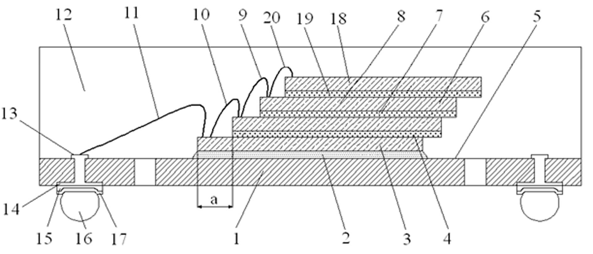
Embodiment 2
[0141] The ultra-thin chip thinning machine of 8 inches and above with fine grinding and polishing functions is used for wafer thinning to obtain a wafer with a final thickness of 110 μm. During the thinning process, the rough grinding range of the wafer is from the original wafer Thickness + film thickness to 175μm + film thickness, coarse grinding speed is 85μm / min, fine grinding range is from 175μm + film thickness to 115μm + film thickness, fine grinding speed is 12μm / min; polishing range is from 115μm + film thickness To 110μm + film thickness, the polishing speed is 0.035μm / s.
[0142] Use the DAD3350 dicing machine to dice the thinned wafer to obtain IC chips; use anti-fragmentation software to control the feed speed of ≤6.5mm / min when dicing; paste an IC chip on the substrate with insulating glue, and then use The adhesive film is stacked and pasted on the IC chip with two layers of IC chips. The two layers of IC chips are all dislocated in the same direction, and the ...
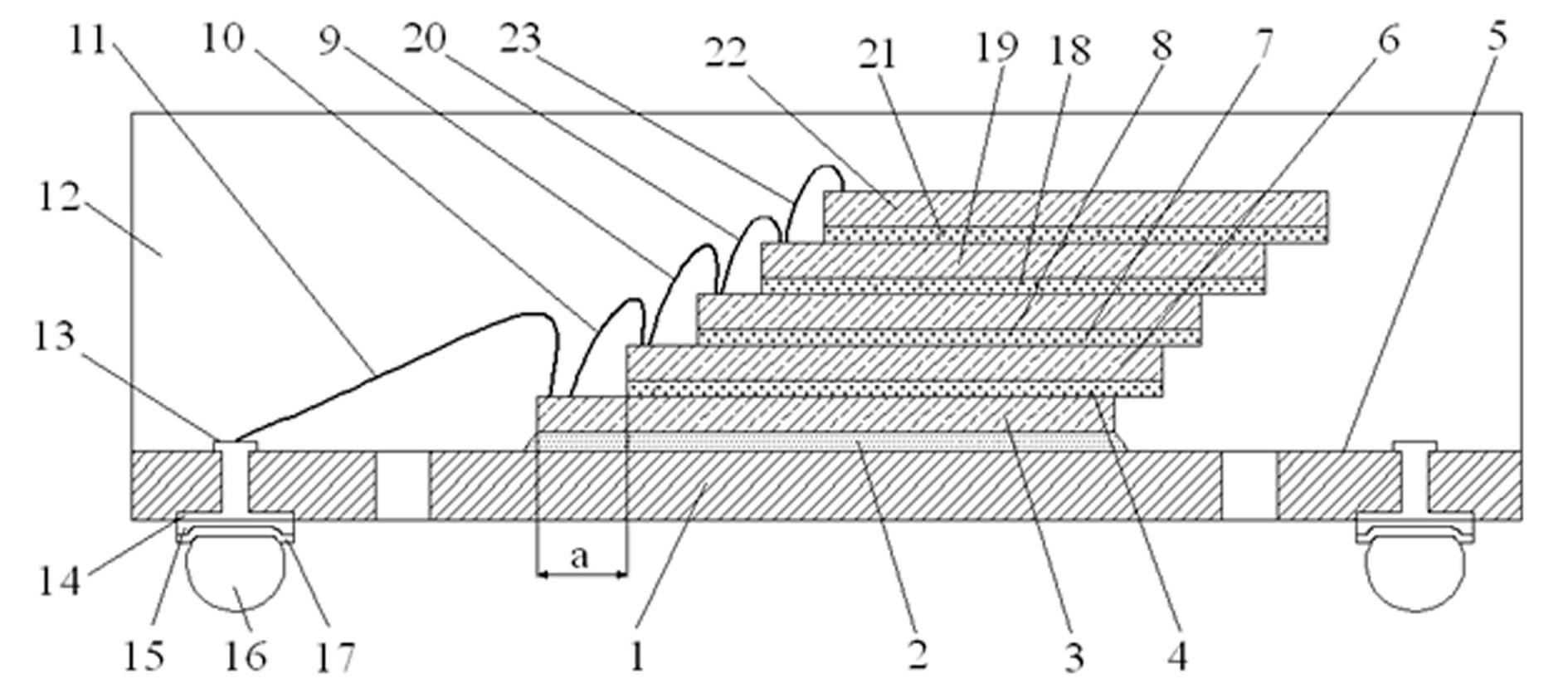
Embodiment 3
[0144] Use an 8-inch and above ultra-thin chip thinning machine with fine grinding and polishing functions for wafer thinning to obtain a wafer with a final thickness of 100 μm: when thinning, the rough grinding range of the wafer is from the original wafer thickness +film thickness to 165μm+film thickness, coarse grinding speed is 120μm / min, fine grinding range is from 165μm+film thickness to 105μm +film thickness, fine grinding speed is 13μm / min; polishing range is from 105μm+film thickness to 100μm + film thickness, fine grinding speed is 0.025μm / s;
[0145]Use A-WD-300TXB dicing machine to dice the thinned wafer to obtain IC chips; use anti-fragmentation software to control the feed speed ≤ 8mm / min during the dicing process; paste an IC on the substrate with insulating glue chip, and then use insulating glue to stack and paste two layers of IC chips on the IC chip. The misalignment distance is 1.43mm; bake at a temperature of 175°C for 3 hours after loading the core. The ...
PUM
 Abstract
Description
Claims
Application Information