Femtosecond laser film micro-nanomachining real-time monitoring device
A technology of micro-nano processing and femtosecond laser, which is applied in the field of micro-processing devices of spectroscopic technology, can solve problems that affect the efficiency and continuity of processing, and cannot meet the needs of precision and miniaturization, so as to improve detection efficiency and reliability. Sexuality, saving processing efficiency, and wide application range
- Summary
- Abstract
- Description
- Claims
- Application Information
AI Technical Summary
Problems solved by technology
Method used
Image

Examples
Embodiment 1
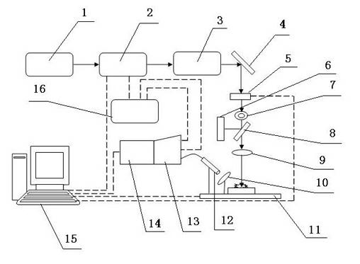
[0018] Embodiment 1, with reference to figure 1 , a femtosecond laser thin film micro-nano processing device, the device includes a laser generating system, an external optical path system, a PC 15 and a three-dimensional mobile platform 11; the laser generating system consists of a pumping source 1, a femtosecond laser 2 and The regenerative amplifier 3 is composed of; the external optical path system is composed of a total reflection mirror 4, an optical gate 5, an attenuation mirror 7, a half-transparent mirror 8 and a focusing mirror 9; the laser emitted by the laser generating system is focused on the external optical path system On the focusing mirror 9; it is characterized in that: the device is also provided with a spectral focusing mirror 10, an optical fiber probe 12, a spectrometer 13, an enhanced CCD14 and a time delay controller 16; the described spectral focusing mirror 10 and the optical fiber probe 12 are fixed on a three-dimensional On the mobile platform 11, ...
Embodiment 2
[0019] Embodiment 2, in the femtosecond laser thin film micro-nano processing device described in Embodiment 1: an energy meter 6 is provided on the reflection direction side of the half mirror 8 .
Embodiment 3
[0020] Embodiment 3, in the femtosecond laser thin film micro-nano processing device described in Embodiment 1 or 2: the response band of the spectrometer is 200nm-980nm, and the resolution is 0.1nm.
[0021] The femtosecond laser thin film micro-nano processing device of this embodiment is used to conduct experiments for processing thin film samples. Before processing monitoring, first open the shutter 5, adjust the attenuation mirror 7, detect the pulse energy through the energy meter 6, and manually adjust the position of the focusing mirror 9, so that the beam is focused on the sample surface placed on the three-dimensional mobile platform 11. Adjust the distance and angle between the spectral focusing mirror 10 and the optical fiber probe 12 and the sample, when the strongest plasma line can be obtained through the spectrometer 13, enhanced CCD14, time delay controller (DG535) 16 and PC 15, Fix the spectral focusing mirror 10 and the optical fiber probe 12 on the surface ...
PUM
 Abstract
Description
Claims
Application Information