PD SOI (partially-depleted silicon on insulator) technology-based body grid coupling ESD (electro-static discharge) protection structure

A protection structure and body gate technology, applied in the field of electrostatic discharge (ESD) protection circuits and semiconductor integrated circuits, can solve problems such as uneven conduction of multi-finger parallel GGNMOS, eliminate the problem of back channel leakage, strong anti-irradiation effect of ability

Active Publication Date: 2012-09-05
西安西岳电子技术有限公司
View PDF2 Cites 18 Cited by
  • Summary
  • Abstract
  • Description
  • Claims
  • Application Information

AI Technical Summary

Problems solved by technology

[0009] The technical problem solved by the present invention is to solve the problem of non-uniform conduction of multi-finger parallel GGNMOS caused by the

Method used


Image

  • PD SOI (partially-depleted silicon on insulator) technology-based body grid coupling ESD (electro-static discharge) protection structure
  • PD SOI (partially-depleted silicon on insulator) technology-based body grid coupling ESD (electro-static discharge) protection structure
  • PD SOI (partially-depleted silicon on insulator) technology-based body grid coupling ESD (electro-static discharge) protection structure

Examples


Embodiment Construction

[0021] Below in conjunction with accompanying drawing, the present invention is described in further detail:

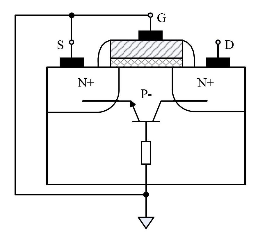
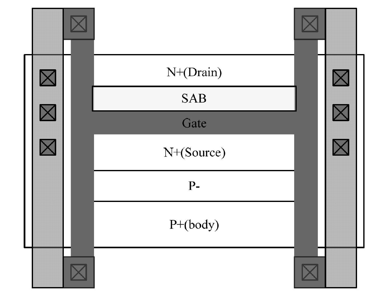
[0022] Such as image 3 , Figure 4 and Figure 5 As shown, a body-gate coupled NMOS ESD protection structure is proposed. In this structure, the gate adopts an H gate structure, and a body implant is performed on the outside and inside of the side gate of the H gate, and the body implant outside the side gate of the H gate is connected to the H gate. Make connections and ground. The source region and the drain region adopt an asymmetric structure of shallow source and deep drain, and the drain region uses the SAB layer to block the silicide to form a ballast resistance, which is conducive to the uniform conduction of multiple parallel tubes. A top view of the structure is image 3 As shown, the cross-sectional view along the source-drain direction is shown in Figure 4 shown.

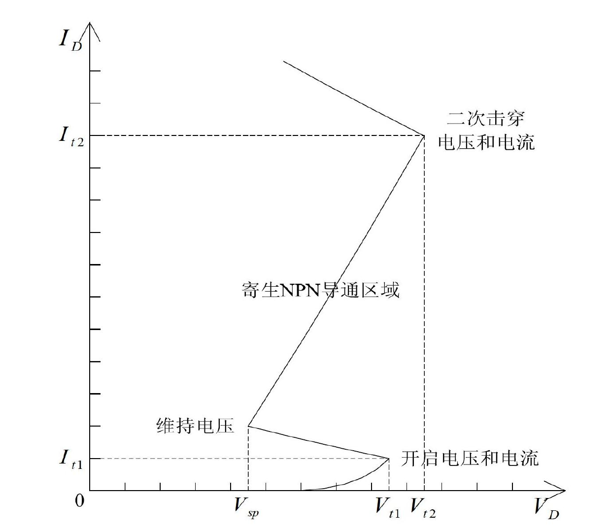
[0023] The equivalent circuit of the body-gate coupled NMOS ESD protection structur...


PUM

PropertyMeasurementUnit
Lengthaaaaaaaaaa

Abstract

The invention discloses a PD SOI (partially-depleted silicon on insulator) technology-based body grid coupling NMOS ESD (n-channel metal oxide semiconductor electro-static discharge) protection structure, wherein a grid electrode in the structure adopts an H-shaped structure, the inner side and the outer side of an edge grid of an H-shaped grid adopt two body region P+ implantation, a drain region adopts N+ deep implantation, a silicon film on an SOI substrate is punched through, a source region adopts N+ shallow implantation, and some silicon film on the SOI substrate adopts the implantation, so that the body region P+ implantation is carried out at the outer side of the source region, and body region contact is led out, and some drain region baffles the silicide by an SAB (salicide block) layer, so that a ballast resistor can be formed. When the protection structure is used, the drain region is connected with a PAD, the body region at the outer side of the edge grid of the H-shaped grid is connected with the grid electrode, and the source region and the body region at the inner side of the H-shaped grid are grounded. According to the protection structure, the body region at the outer side of the edge grid of the H-shaped grid is connected with the grid electrode, so that a coupling circuit can be formed by sufficiently using a parasitic capacitor of a drain body and a parasitic resistor of a body region under the source region, and the grid electrode is coupled with a certain voltage, so that the starting voltage of the ESD protection structure can be reduced, the even conduction of the plurality of structures can be guaranteed, and the ESD protection capability can be improved.

Description

technical field [0001] The invention relates to the field of semiconductor integrated circuits, in particular to the field of electrostatic discharge (ESD) protection circuits based on PD SOI CMOS technology. Background technique [0002] With the continuous improvement of the integrated circuit manufacturing process, the length of the polysilicon gate is getting smaller and smaller, the thickness of the gate oxide is getting thinner, and the junction depth is getting shallower and shallower. The gate oxide breakdown, PN junction thermal breakdown, The problems of interconnection burning and potential damage are becoming more and more serious. ESD has become an urgent reliability problem in the field of integrated circuits. Therefore, ESD protection circuits have become the focus of research on the reliability of CMOS integrated circuits. Because SOI CMOS devices have the advantages of low power consumption, strong anti-interference ability, high integration, fast speed, str...

Claims


Application Information

Patent Timeline
IPC IPC(8): H01L27/02
Inventor 王忠芳谢成明李海松赵德益吴龙胜刘佑宝
Owner 西安西岳电子技术有限公司
Why Eureka
Try Eureka