Die attach film

A technology for attaching and chipping, applied in the direction of film/sheet adhesive, epoxy resin glue, adhesive type, etc., can solve the problems of reduced embedding of semiconductor substrates, reduced reliability of semiconductor packaging, etc., and achieves excellent Effects of expansion and pickup characteristics, prevention of burrs or flying chips, and improvement of embedability

Active Publication Date: 2012-09-05
LG CHEM LTD
View PDF4 Cites 6 Cited by
  • Summary
  • Abstract
  • Description
  • Claims
  • Application Information

AI Technical Summary

Problems solved by technology

However, when the pre-curing process is performed, the adhesive starts to cure, so in the subsequent process, the embedding property for the semiconductor substrate is lowered
In addition, due to the heat applied in the pre-curing process, the wafer or substrate becomes warped, so failures such as pop-up may occur when performing wire bonding
Like this, there is a possibility that the reliability of the semiconductor package will be greatly reduced

Method used


Image

  • Die attach film
  • Die attach film
  • Die attach film

Examples


preparation example 1

[0093] Preparation Example 1: Preparation of high molecular weight resin with low elasticity

[0094] 100 parts by weight of butyl acrylate, 100 parts by weight of ethyl acrylate, 70 parts by weight of acrylonitrile, 8 parts by weight of glycidyl methacrylate, 4 parts by weight of acrylic acid and 750 parts by weight of deionized distilled water were added to In a four-port 3L reactor with a stirrer, nitrogen replacement device and thermometer. Then, 2 parts by weight of suspending agent (polyvinyl alcohol (trademark: NH-17, produced by Nippon Ghosei) diluted with water to 4%) and 0.3 parts by weight of molecular weight regulator (dodecyl mercaptan) were added, To make a mixture. The resulting mixture was subjected to a nitrogen replacement process for about 1 hour, and then heated to 55°C. When the temperature reaches the preset temperature, 2 parts by weight of bis(ethylhexyl) peroxydicarbonate (trademark: Trigonox EHP, produced by Akzo Nobel) diluted with ethyl acetate to a ...

Embodiment 1

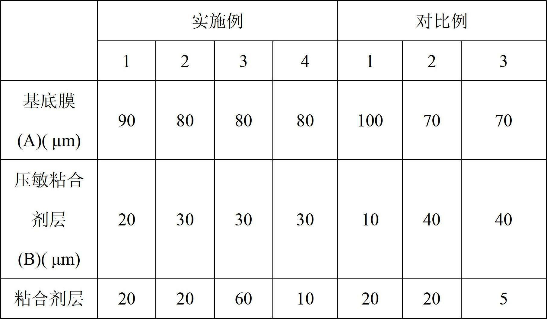
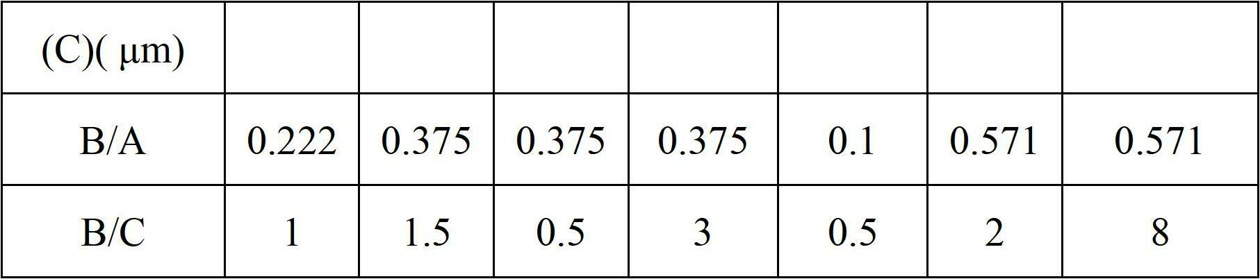
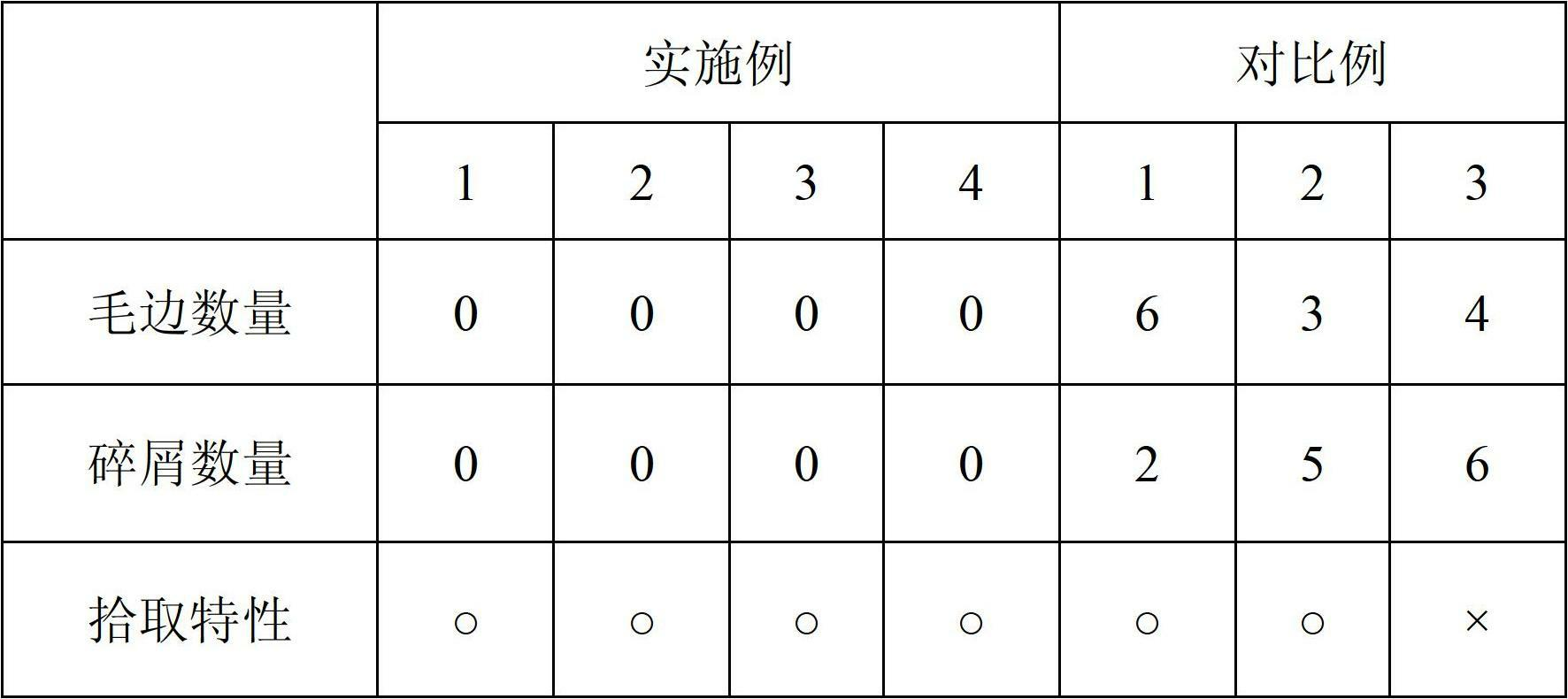
[0095] Example 1: Preparation of dicing film (pressure sensitive adhesive film)

[0096] With respect to 100 parts by weight of the multifunctional oligomer, 7 parts by weight of Darocur TPO as a photoinitiator and 100 parts by weight of acrylic copolymer, 5 parts by weight of isocyanate hardener and 10 parts by weight of isocyanate hardener are mixed with a weight average molecular weight of 20,000. A mixture of polyfunctional oligomers, to prepare a UV (ultraviolet light) curable pressure-sensitive adhesive composition, the acrylic copolymer is obtained by making 2-ethylhexyl acrylate, methyl acrylate and methacrylic acid It is made by copolymerization of methyl ester and has a weight average molecular weight of 800,000 and a glass transition temperature of 10°C. Then, the above-mentioned UV curable pressure-sensitive adhesive composition was coated on a polyester film that had been subjected to a release treatment and had a thickness of 38 μm so as to have a thickness of 20 μm...

Embodiment 2

[0100] The die attach film was produced in the same manner as in Example 1, except that the pressure-sensitive adhesive film was prepared by controlling the pressure-sensitive adhesive layer to have a thickness of 30 μm and using a polyolefin film having a thickness of 80 μm.


PUM

PropertyMeasurementUnit
thicknessaaaaaaaaaa
thicknessaaaaaaaaaa
glass transition temperatureaaaaaaaaaa

Abstract

The present invention relates to a die attach film, a semiconductor wafer, and a semiconductor packaging method. The invention provides a die attach film, which can prevent chip scattering or generation of burrs or the like during a dicing process and shows excellent expandability and pickup effect when a die bonding process is performed. Further, according to the present invention, the die attach film is capable of preventing chips from being detached, pushed out or deflected during a wire bonding or molding process. Thus, the invention improves the embedding property, suppresses the warpage of a wafer or a wiring substrate, and enhances productivity during a semiconductor package process.

Description

Technical field [0001] The invention relates to a die attach film (die attach film), a semiconductor wafer (semiconductor wafer) and a semiconductor packaging method. Background technique [0002] As semiconductor memories used in mobile phones or mobile terminals tend to be highly integrated and functional, a method of stacking a plurality of semiconductor chips on a semiconductor substrate with a chip attach film has been often used. [0003] The die attach film includes a pressure-sensitive adhesive layer for fixing a semiconductor wafer during a dicing process, and a die attaching process that is adhered to the back surface of the semiconductor wafer and attached to a wiring substrate (such as a lead frame) Adhesive layer. [0004] The packaging process using die attach film usually includes: a dicing process of dicing the wafer into individual wafers, a die bonding process of bonding the diced wafer to a circuit film or lead frame, using electrical connection methods (such as m...

Claims


Application Information

Patent Timeline
Patent Type & Authority Applications(China)
IPC IPC(8): H01L21/58C09J7/20
CPCC08G2650/40C09J163/00C09J2203/326C09J2463/00H01L21/6836H01L24/83H01L24/85H01L2221/68327H01L2224/27436H01L2224/83191H01L2224/8385H01L2924/01005H01L2924/01012H01L2924/01013H01L2924/01033H01L2924/0106H01L2924/01082H01L2924/07802H01L2224/2919H01L2924/01006H01L2924/0102H01L2924/0104H01L2924/0665H01L24/29H01L2224/85H01L2924/10253H01L2924/00014H01L2224/451H01L2924/181C08L71/00C08L79/08C08L81/06C09J7/20Y10T428/24959C09J2301/208C09J2301/304C09J2301/302H01L2924/00H01L2924/3512H01L2224/48H01L2224/45099
Inventor 朱孝叔张锡基朴孝淳洪宗完赵显珠金章淳朴容秀
Owner LG CHEM LTD
Why Eureka
Try Eureka