Building method of gallium arsenide field-effect tube (GaAs FET) temperature influence model

A gallium arsenide field and influence model technology, applied in the field of microelectronics, can solve the problems of unpredictable performance parameters and temperature influence, and does not reveal the physical mechanism of temperature influence, so as to achieve the effect of good portability

Inactive Publication Date: 2012-09-12
BEIHANG UNIV
View PDF4 Cites 12 Cited by
  • Summary
  • Abstract
  • Description
  • Claims
  • Application Information

AI Technical Summary

Problems solved by technology

When characterizing the degree to which model parameters are affected by temperature, these empirical analysis models all use the method of numerical fitting to the measured data, but do not reveal the physical mechanism of temperature influence, so it cannot be predicted before the device is manufactured and measured Its performance parameters and temperature influence

Method used


Image

  • Building method of gallium arsenide field-effect tube (GaAs FET) temperature influence model
  • Building method of gallium arsenide field-effect tube (GaAs FET) temperature influence model
  • Building method of gallium arsenide field-effect tube (GaAs FET) temperature influence model

Examples


Embodiment Construction

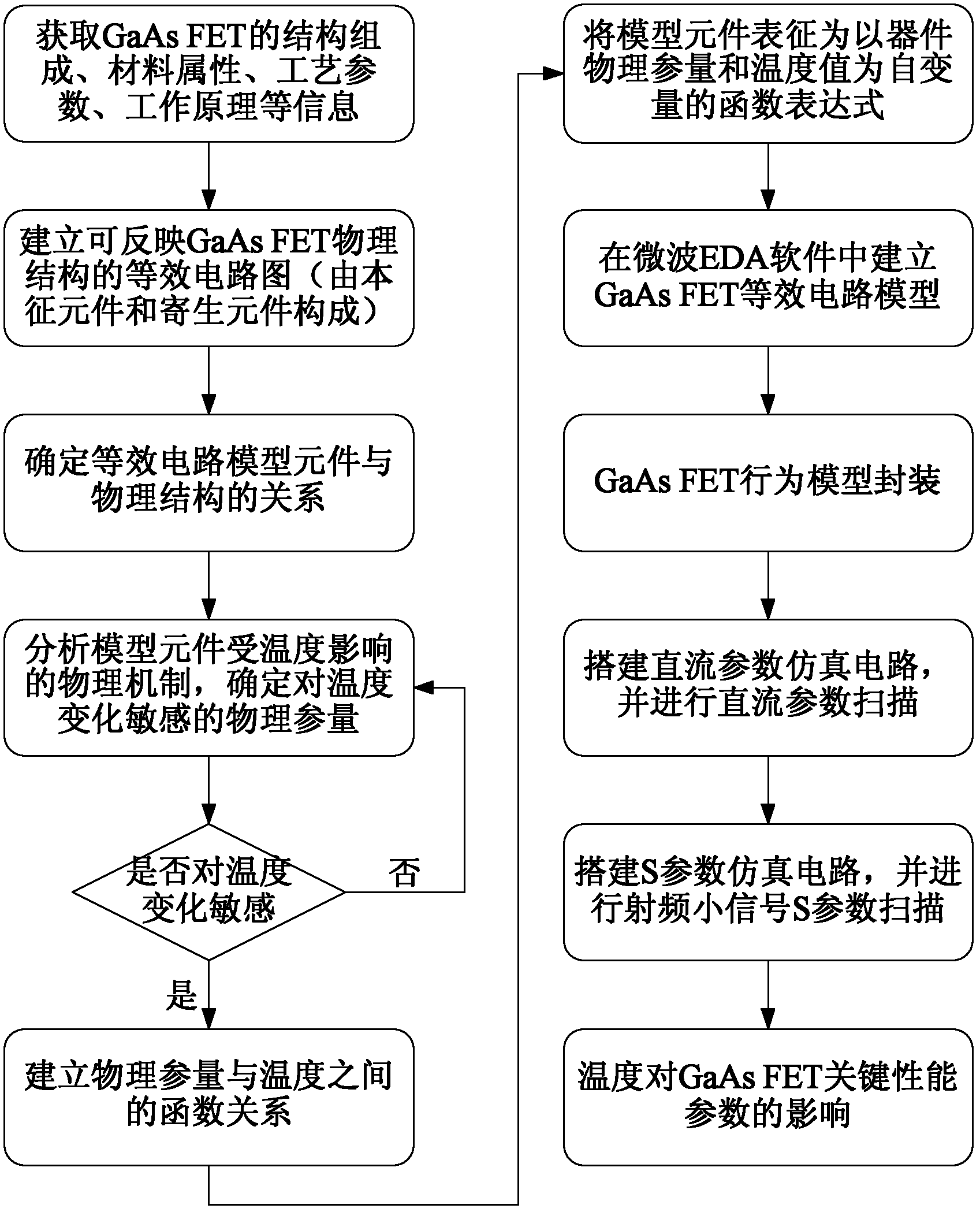
[0035] The method for establishing the temperature influence model of GaAs FET according to the present invention will be described in detail below in combination with specific implementation cases.

[0036] Case: An ion-implanted GaAs FET with a gate length of 1 μm, a gate-source spacing of 1 μm, a gate width of 300 μm, and an active layer doping concentration of 1.0×10 17 cm -3 , the thickness of the active layer is 0.2 μm, the thickness of the gate metal is 0.5 μm, and the gate metal is Au.

[0037] See figure 1 , a method for establishing a GaAs field effect transistor temperature influence model of the present invention, the specific steps of the method are as follows:

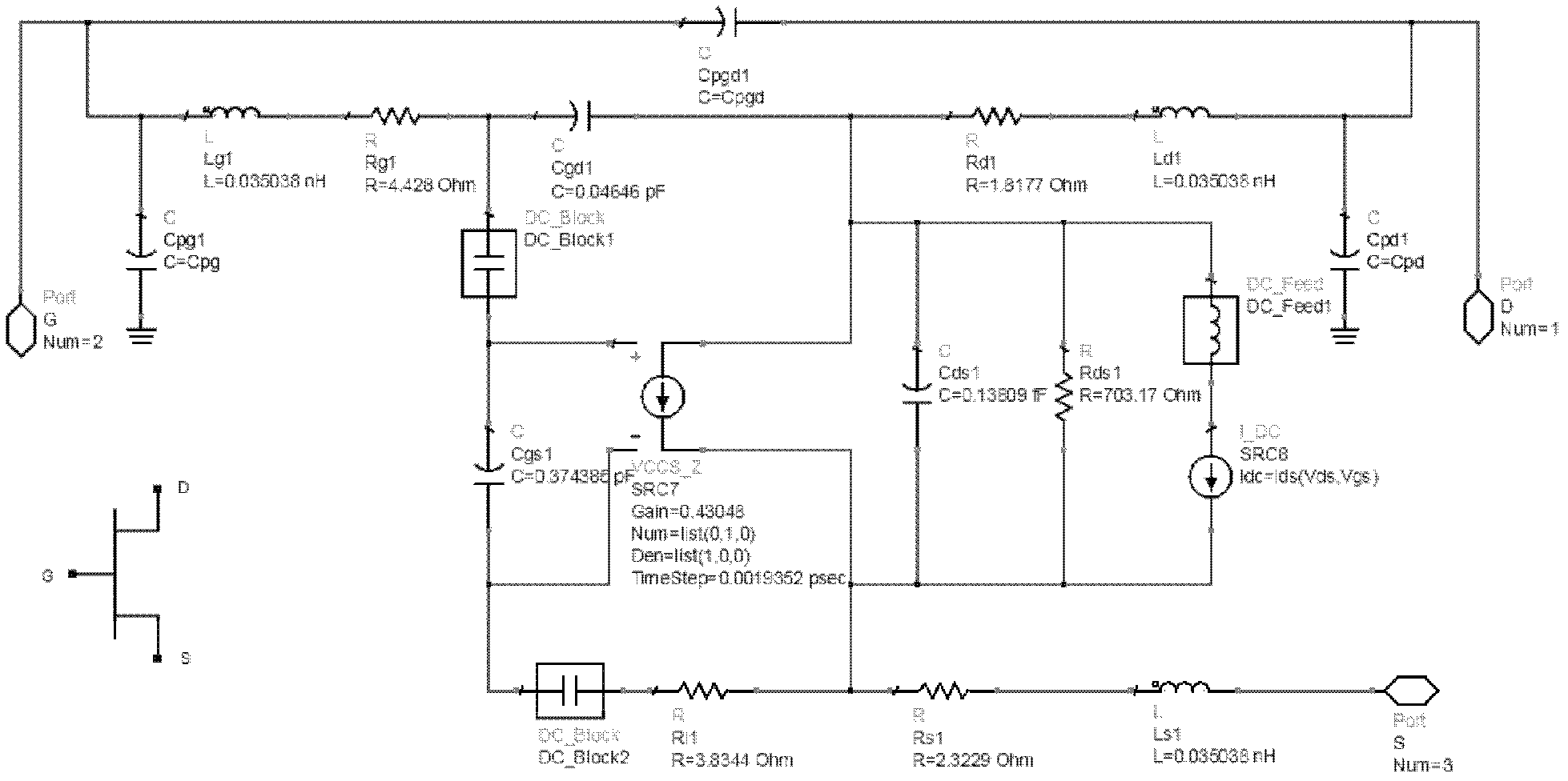
[0038] Step 1: There are many kinds of GaAs FET equivalent circuit diagrams. Here, a more mature Curtice model is selected, and parasitic inductance and parasitic pad capacitance are added on this basis.

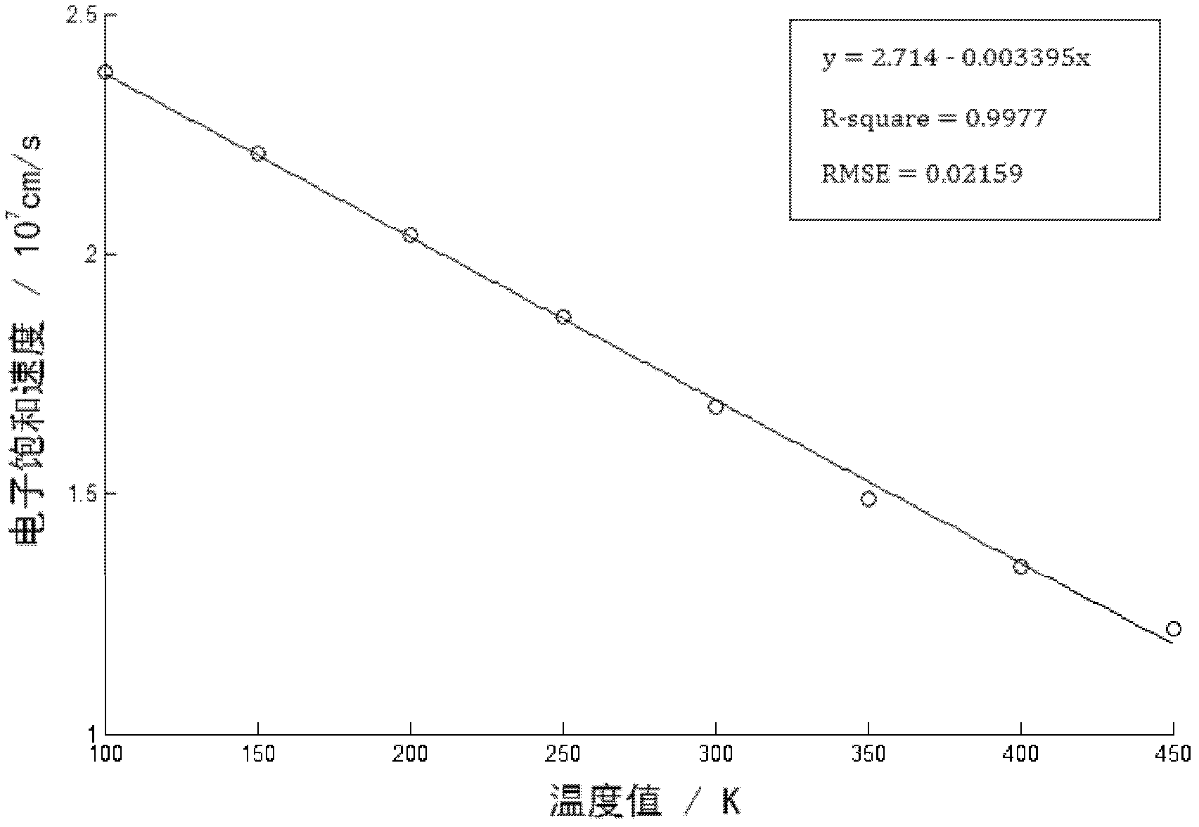
[0039] Step 2: When performing DC parameter analysis, the drain current I ds The Statz-Pucel mod...


PUM


Abstract

The invention relates to a building method of a gallium arsenide field-effect tube (GaAs FET) temperature influence model. The method comprises the following steps of: 1, building an equivalent circuit diagram capable of reflecting a GaAs FET physical structure; 2, determining the relationship between an equivalent circuit model element and the physical structure; 3, studying and determining the temperature influence physical mechanism of the model element; 4, building the function relationship between the model element and the temperature; 5, realizing the GaAs FET equivalent circuit model in microwave electronic design automation (EDA) software; and 6, simulating the GaAs FET critical performance parameter change relationship along with the temperature. The building method can simulate the relationship between the GaAs FET performance parameters and the physical structure, the temperature influence on the GaAs FET performance parameters can be predicted, and the structure design and technological parameter optimization can be conveniently performed by device design personnel. The building method has a better practical value and a good application prospect in the microelectronic technical field.

Description

technical field [0001] The invention relates to a method for establishing a temperature influence model of a gallium arsenide field effect transistor (GaAs FET), which is an equivalent circuit model realization method in the field of simulation analysis of microwave power devices, and is dedicated to characterizing the temperature of GaAs FET key performance parameters Influence, to evaluate its parameter degradation degree in high temperature environment, in order to reduce the application risk, belongs to the field of microelectronics technology. Background technique [0002] GaAs FETs have the advantages of low noise figure, wide frequency band, strong radiation resistance and high power-added efficiency, and are widely used in T / R components that constitute active phased array radars. The performance of GaAs FET is greatly affected by temperature. When the temperature changes, its electrical characteristics will change accordingly. For example, the transconductance will...

Claims


Application Information

Patent Timeline
Patent Type & Authority Applications(China)
IPC IPC(8): G06F17/50
Inventor 张超付桂翠谷瀚天张栋
Owner BEIHANG UNIV
Why Eureka
Try Eureka