Supercharge Your Innovation With Domain-Expert AI Agents!

Preparation method of double-layer silicon-on-insulator (SOI) mixed crystal orientation back-grid type transoid mode Si nanowire field effect transistor (NWFET)

A mixed crystal orientation and double-layer technology, applied in semiconductor/solid-state device manufacturing, nanotechnology for information processing, electrical components, etc., can solve the problem of gate resistivity adjustment, difficult process, and inability to adjust gate work function and other problems, to achieve the effect of convenient implementation, high device integration, and easy silicon layer peeling

Active Publication Date: 2014-07-16
SHANGHAI HUALI MICROELECTRONICS CORP
View PDF6 Cites 0 Cited by
  • Summary
  • Abstract
  • Description
  • Claims
  • Application Information

AI Technical Summary

Problems solved by technology

[0009] The present invention is aimed at the prior art, the existing semiconductor nanowire MOSFET can not realize the separation structure of NMOS and PMOS, can not adjust the gate work function and the gate resistivity for NMOS and PMOS respectively, and realize the separate structure for NMOS and PMOS The process of source-drain ion implantation is difficult and other defects Provide a preparation method for double-layer isolation mixed crystal orientation gate-back inversion mode SiNWFET on SOI

Method used


Image

  • Preparation method of double-layer silicon-on-insulator (SOI) mixed crystal orientation back-grid type transoid mode Si nanowire field effect transistor (NWFET)
  • Preparation method of double-layer silicon-on-insulator (SOI) mixed crystal orientation back-grid type transoid mode Si nanowire field effect transistor (NWFET)
  • Preparation method of double-layer silicon-on-insulator (SOI) mixed crystal orientation back-grid type transoid mode Si nanowire field effect transistor (NWFET)

Examples


preparation example Construction

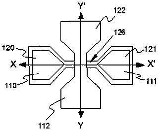
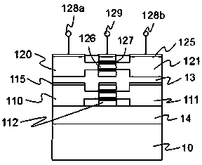
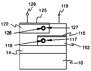
[0045] The invention provides a method for preparing a double-layer SOI mixed crystal orientation gate-back type inversion mode SiNWFET. That is, the channel regions of the upper and lower layers of MOSFETs are silicon nanowires with different surface orientations. In the low-temperature lift-off technology, as the hydrogen pressure increases, cracks tend to grow along the (100) crystal direction, so it is easier to peel off the silicon layer along the (100) crystal direction, so the lower PMOSFET + upper NMOSFET mode is used.

[0046] Theoretically speaking, the upper and lower layers of SiNWFETs can use silicon nanowires with any surface orientation. According to the research results of Yang M et al., (100) / has the largest electron mobility, and (110) / maximum hole mobility. Therefore, preferably, we use silicon nanowires with (100) surface orientation as the channel material of NMOSFET, and the channel direction of NMOSFET is , and use silicon nanowires with (110) surface...


PUM


Abstract

The invention provides a preparation method of a double-layer silicon-on-insulator (SOI) mixed crystal back-grid type transoid mode Si nanowire field effect transistor (NWFET). A power metal oxide semiconductor field effect transistor (PMOSFET) adopts a (110) surface crystal orientation silicon layer, and an N-type metal oxide semiconductor field effect transistor (NMOSFET) adopts a (100) surface crystal orientation silicon layer. In low temperature peeling technology, cracks are inclined to grow along the crystal orientation with increase of hydrogen pressure, therefore silicon layer peeling can be easily conducted along the (100) crystal orientation, and the layer transfer process is facilitated.

Description

technical field [0001] The invention relates to the technical field of semiconductor field effect transistors, in particular to a preparation process step of an SOI double-layer mixed crystal orientation gate-back type inversion mode SiNWFET. Background technique [0002] It has always been the goal pursued by the development of microelectronics industry to increase the working speed and integration of chips and reduce the power consumption density of chips by reducing the size of transistors. In the past forty years, the development of microelectronics industry has been following Moore's Law. At present, the physical gate length of field effect transistors is close to 20nm, and the gate dielectric is only a few layers thick of oxygen atoms. It is difficult to improve the performance by reducing the size of traditional field effect transistors, mainly because of the short channel Channel effect and gate leakage current deteriorate the switching performance of the transistor...

Claims


Application Information

Patent Timeline
Patent Type & Authority Patents(China)
IPC IPC(8): H01L21/84H01L21/335B82Y10/00
Inventor 黄晓橹
Owner SHANGHAI HUALI MICROELECTRONICS CORP
Features
  • R&D
  • Intellectual Property
  • Life Sciences
  • Materials
  • Tech Scout
  • Unparalleled Data Quality
  • Higher Quality Content
  • 60% Fewer Hallucinations
Learn More