Preparation method of N-type crystalline silicon double-sided back contact solar cell

A technology of solar cells and crystalline silicon, applied in the field of solar cells, can solve problems such as hot spots, inability to diffuse in designated areas, and affect power generation and life of components, and achieve the effects of simple preparation process, good electrical performance, and easy operation

Inactive Publication Date: 2012-09-19
CSI CELLS CO LTD +1
View PDF3 Cites 18 Cited by
  • Summary
  • Abstract
  • Description
  • Claims
  • Application Information

AI Technical Summary

Problems solved by technology

The back electric field of existing N-type back-contact crystalline silicon solar cells is usually formed by the diffusion process of phosphorus oxychloride, and phosphorus oxychloride is carried by nitrogen gas for diffusion, which cannot diffuse in a designated area, so heavy doping cannot be avoided The connection between the doped P-type region and the heavily doped N-type region, and leakage
The leakage of solar cells will lead to hot spots in the subsequent production of components, which will affect the power generation and life of components

Method used


Image

  • Preparation method of N-type crystalline silicon double-sided back contact solar cell
  • Preparation method of N-type crystalline silicon double-sided back contact solar cell
  • Preparation method of N-type crystalline silicon double-sided back contact solar cell

Examples


Embodiment 1

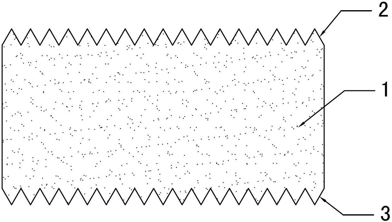
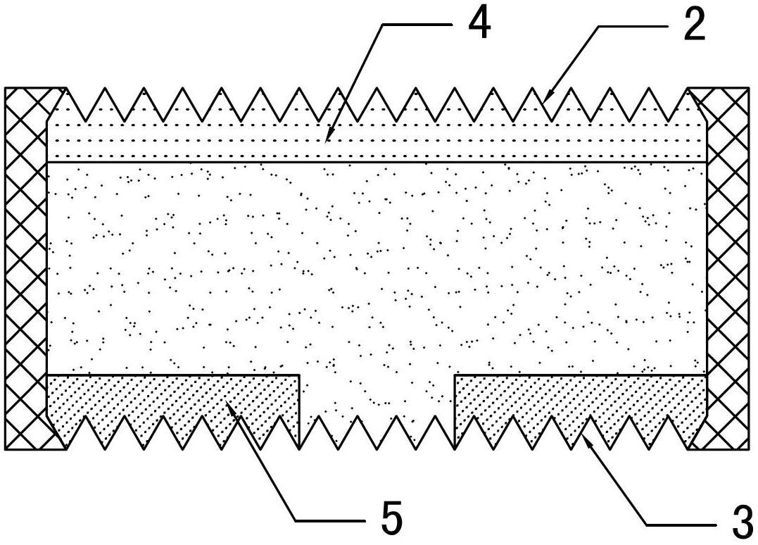
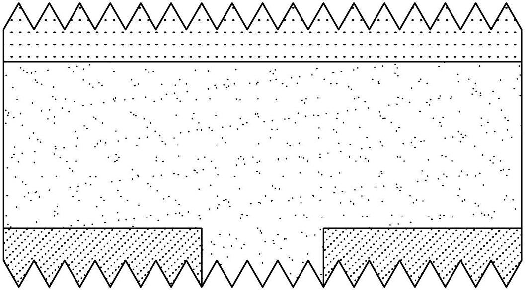
[0038] See Figure 1~7 As shown, a method for preparing an N-type crystalline silicon double-sided back contact solar cell includes the following steps:

[0039] Step S101: performing double-sided texturing on the N-type crystalline silicon wafer 1;

[0040] In the embodiment of the present invention, the contamination and damage layer on the surface of the N-type crystalline silicon wafer is chemically removed, and a suede structure is formed on both the front surface 2 and the back surface 3. The purpose is to reduce the reflection of incident light on the surface of the silicon wafer and increase The absorption of incident light by the silicon wafer; the structure diagram of the N-type crystal silicon wafer after texturing is as follows figure 1 Shown

[0041] Step S102: perform boron doping and local phosphorus doping on the front and back sides of the N-type silicon wafer, respectively;

[0042] By means of high temperature diffusion and other methods, boron doping on the front s...


PUM


Abstract

The invention discloses a preparation method of an N-type crystalline silicon double-sided back contact solar cell, which comprises the following steps of: (1) cleaning and velvet-making; (2) carrying out local phosphorus doping on the back surface of a silicon chip; (3) carrying out boron diffusion on the front surface of the silicon chip; (4) etching a peripheral junction; (5) passivating the front surface and the back surface of the silicon chip or the front surface of the silicon chip; (6) arranging antireflective films on the front surface and the back surface of the silicon chip; (7) forming a hole on the silicon chip; (8) arranging a hole metal electrode in the hole; and printing metal electrodes on the double sides and sintering to obtain the N-type crystalline silicon double-sided back contact solar cell. The preparation method has the advantages that the local phosphorus doping is carried out on the back surface of the silicon chip, a non-phosphorus doping area on the back surface of the silicon chip is a peripheral area of a hole to be formed on the silicon chip, and the problems of short circuit and electricity leakage at the diffused junction are avoided in the solar cell obtained by the preparation method, so that the remarkable effect is obtained.

Description

Technical field [0001] The invention relates to a method for preparing an N-type crystalline silicon double-sided back contact solar cell, which belongs to the field of solar cells. Background technique [0002] Conventional fossil fuels are increasingly depleted. Among the existing sustainable energy sources, solar energy is undoubtedly the cleanest, most common and most potential alternative energy source. At present, among all solar cells, crystalline silicon solar cells are one of the solar cells that have been widely promoted. This is because silicon materials have extremely rich reserves in the earth’s crust. At the same time, silicon solar cells are compared with other types of solar cells. , Has excellent electrical and mechanical properties. Therefore, crystalline silicon solar cells occupy an important position in the photovoltaic field. High efficiency is the current development trend of crystalline silicon solar cells. The conversion efficiency of solar cells is imp...

Claims


Application Information

Patent Timeline
Patent Type & Authority Applications(China)
IPC IPC(8): H01L31/18
CPCY02P70/50
Inventor 杨智王栩生章灵军
Owner CSI CELLS CO LTD
Why Eureka
Try Eureka