

Charge regeneration structure, its preparation method and application
A charge and electron transport technology, applied in the direction of chemical instruments and methods, circuits, electrical components, etc., can solve the problem of high starting voltage of light-emitting devices, and achieve the effects of avoiding interface defects, low cost, and simple operation
- Summary
- Abstract
- Description
- Claims
- Application Information
AI Technical Summary
Problems solved by technology
Method used
Image

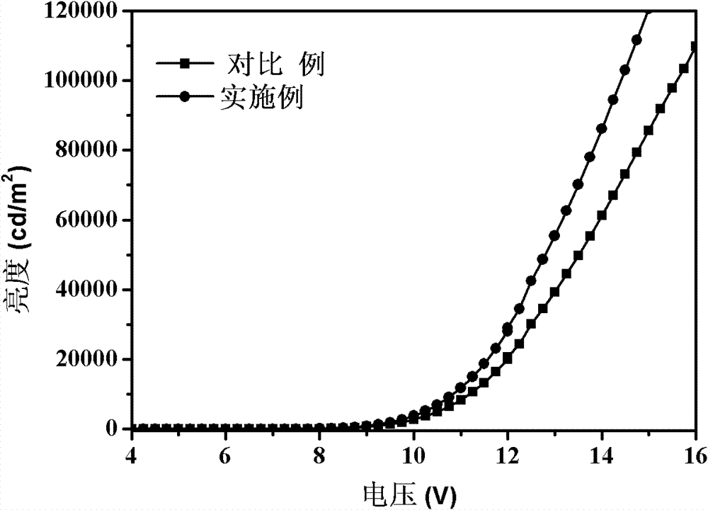
Examples
preparation example Construction
[0044] The embodiment of the present invention further provides a method for preparing the above-mentioned charge regeneration structure, including the following steps:
[0045] Mixing a p-type semiconductor material, an organic material with electron transport capability, and an n-type semiconductor material to obtain a mixture, the homo energy level of the p-type semiconductor material is greater than 5.0, and the weight percentage is 10-40%; the n-type semiconductor material The weight percentage of the material is 30-50%;
[0046] The mixture is vapor-deposited, sputtered or spin-coated to form a charge regeneration structure.
[0047] Specifically, in the preparation method of the charge regeneration structure in the embodiment of the present invention, the evaporation, sputtering, or spin coating method used is not specifically limited, and the substrate used in evaporation, sputtering, or spin coating is the one using the charge regeneration structure The light-emittin...
Embodiment 1
[0057] The method for preparing an organic electroluminescent device according to an embodiment of the present invention includes the following steps:
[0058] Prepare the first light-emitting unit:
[0059] Evaporate on ITO glass, form (molybdenum trioxide) hole injection layer, evaporate on this hole injection layer, form (Alq 3 ) a light-emitting layer, vapor-deposited on the light-emitting layer to form a (PBD) electron transport layer;
[0060] Prepare the charge regeneration structure:
[0061] Mix molybdenum trioxide, Bphen, and cesium azide to obtain a mixture, the weight percentage of the molybdenum trioxide is 20%; the weight percentage of the cesium azide is 40%, and then the mixture is placed in the first light-emitting unit Evaporation is carried out on the electron transport layer to form a charge regeneration structure with a thickness of 15 nanometers;
[0062] Preparation of the second light-emitting unit:
[0063] Evaporate and form (NPB) hole transport l...
Embodiment 2
[0067] The method for preparing an organic electroluminescent device according to an embodiment of the present invention includes the following steps:
[0068] Prepare the first light-emitting unit:
[0069] Sputtering on ITO glass, forming (molybdenum trioxide) hole injection layer, vapor deposition on the hole injection layer, forming (NPB) hole transport layer, sputtering on the hole transport layer, forming (NPB ) electron blocking layer, sputtering on the electron blocking layer, forming (AND) light-emitting layer, evaporation on the light-emitting layer, forming (Alq 3 ) hole blocking layer, sputtering on the hole blocking layer, forming (Alq 3 ) electron transport layer;
[0070] Prepare the charge regeneration structure:
[0071] Molybdenum trioxide, BALQ, cesium azide are mixed to obtain a mixture, the molybdenum trioxide is 10% by weight relative to the BALQ; the cesium azide is 20% by weight relative to the BALQ, and then The mixture is sputtered on the electron...
PUM
| Property | Measurement | Unit |
|---|---|---|
| thickness | aaaaa | aaaaa |
| thickness | aaaaa | aaaaa |
| thickness | aaaaa | aaaaa |
Abstract
Description
Claims
Application Information