Thin film filling method

A filling method and thin film technology, which is applied in coating, gaseous chemical plating, metal material coating process, etc., can solve the problems of high leakage current path of devices, device failure, yield reduction, etc., and achieve the effect of good filling effect

Inactive Publication Date: 2012-09-26
INST OF MICROELECTRONICS CHINESE ACAD OF SCI
View PDF3 Cites 16 Cited by
  • Summary
  • Abstract
  • Description
  • Claims
  • Application Information

AI Technical Summary

Problems solved by technology

[0006] However, if there are holes in the film filling of trenches or gaps, the interconnection metal in the subsequent process may fill into these holes, causing a high leakage current path between devices, resulting in device failure and reduced yield.

Method used


Image

  • Thin film filling method
  • Thin film filling method
  • Thin film filling method

Examples


Embodiment 1

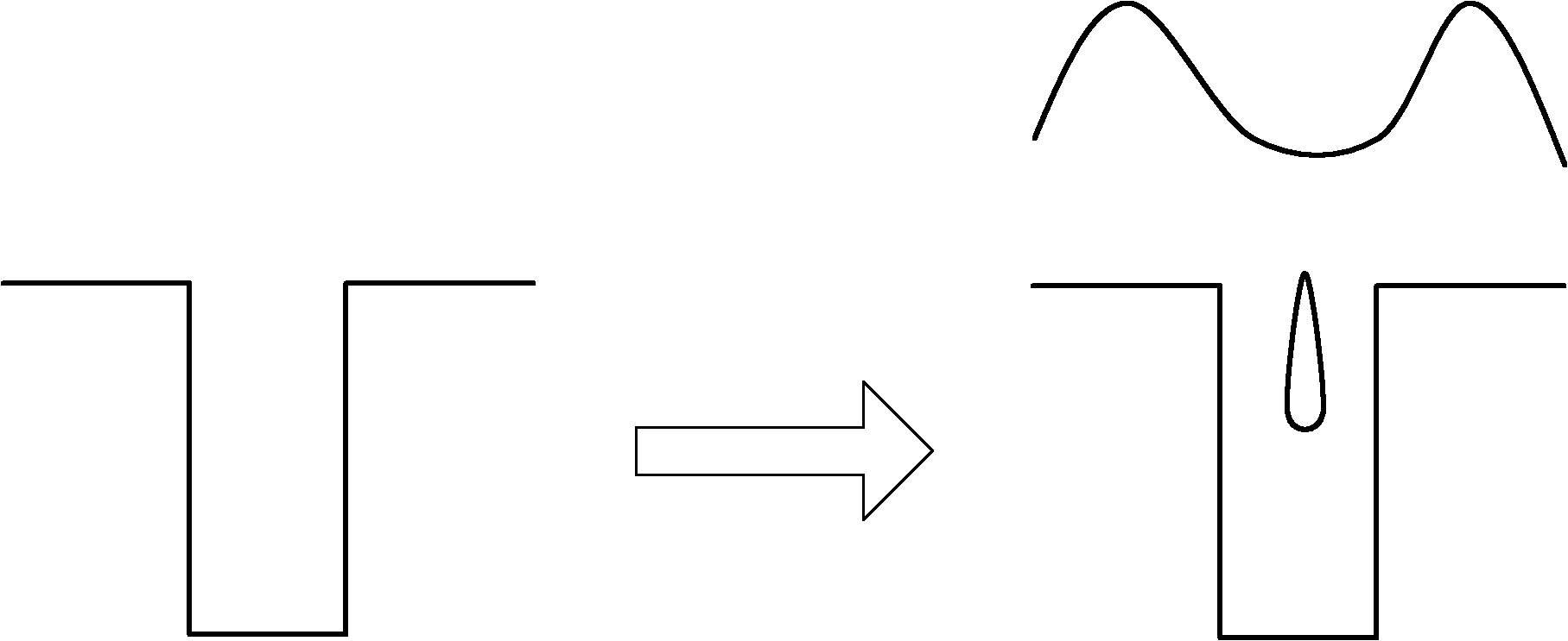
[0071] Such as Figure 4As shown in 401 in a, it is an STI structure formed on the surface of the substrate, which omits the pad oxide layer and nitride layer film grown in the furnace tube and the film oxide layer grown in the gap, and enters after heat treatment and annealing The HDP CVD chamber starts the first part of the deposition. For ease of description, this figure only shows an STI structure, and the formation of the STI structure and active region can refer to the existing conventional technology, which is not limited in the present invention. The semiconductor substrate may include any suitable semiconductor substrate material, specifically, but not limited to, silicon, germanium, silicon germanium, SOI (silicon on insulator), silicon carbide, gallium arsenide, or any III / V compound semiconductor, etc. .

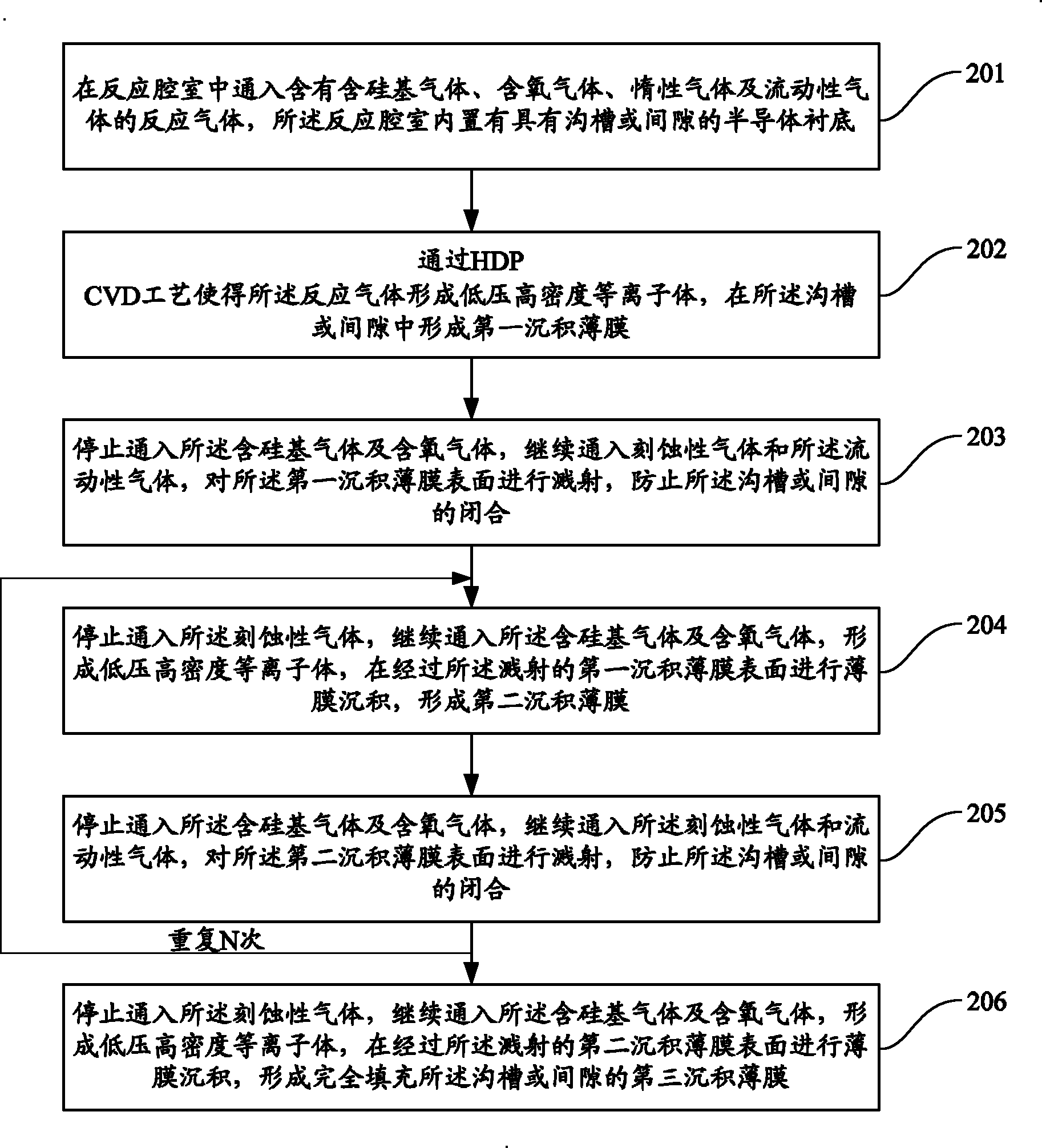
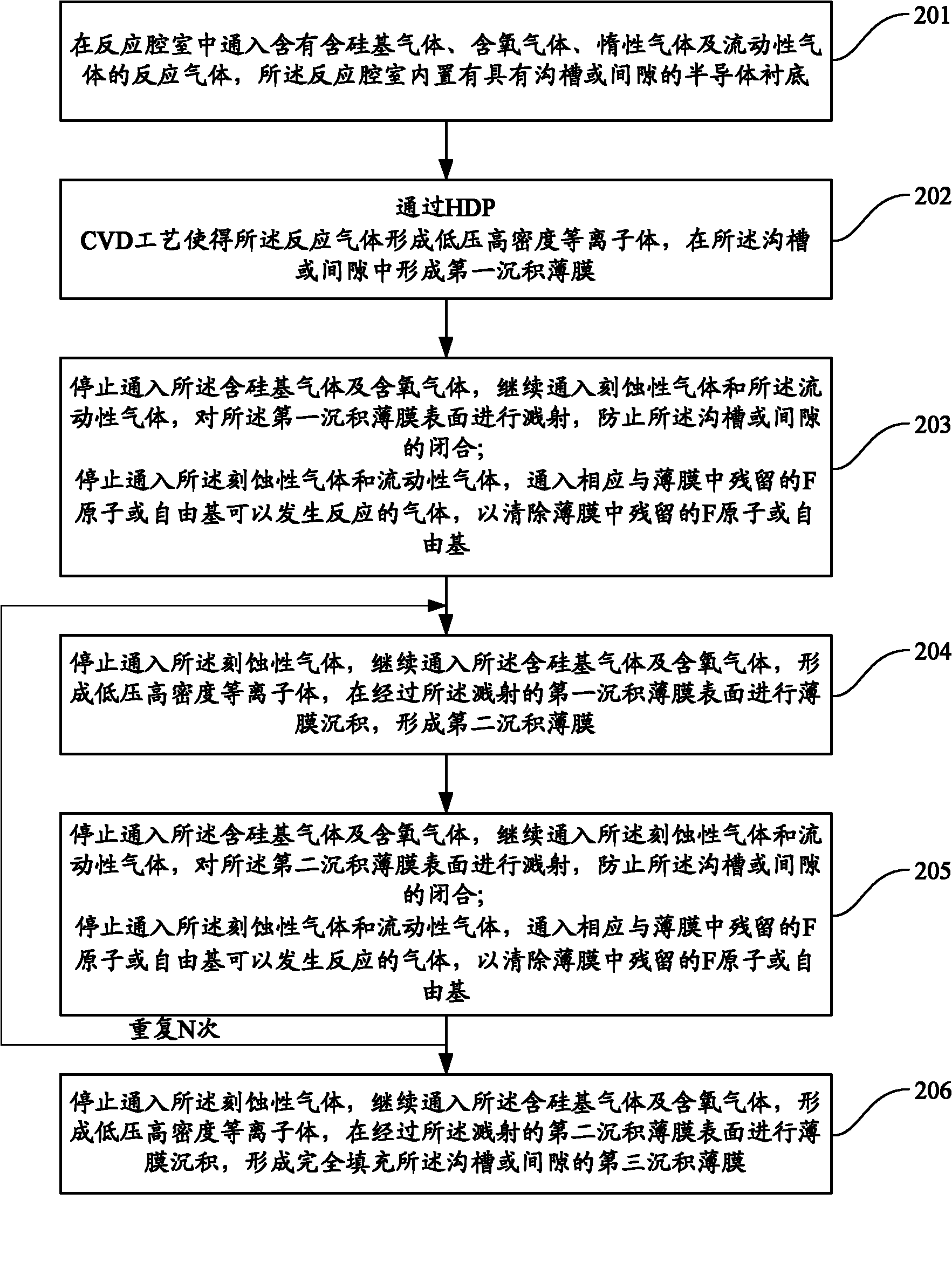
[0072] Figure 5 then shows the Figure 4 The process flow for thin film filling of the STI structure shown specifically includes the following steps:

[00...

Embodiment 2

[0082] Image 6 Another process flow for thin film filling of the STI structure is shown, which specifically includes the following steps:

[0083] Step 601, putting the semiconductor substrate with STI structure into the reaction chamber;

[0084] Step 602, injecting SiH into the reaction chamber 4 , O 2 , He and mobile dilution gas H 2 ;

[0085] Step 603, generating high-density plasma by inductive coupling, and performing ion bombardment under the action of bias power, so that the first deposited film is deposited on the STI and the surface of the substrate;

[0086] In this step, S / D has a lower value, so as to increase the deposition rate as much as possible, so that the film grows from bottom to top in the gap without closing the opening.

[0087] Step 604, stop feeding SiH 4 and O 2 , enter H 2 with NF 3 The physical and chemical etching process under the action;

[0088] The difference from Example 1 is that the etching gas in this example increases NF 3 , ...

no. 3 example

[0093] Figure 7 Another process flow for thin film filling of the STI structure is shown, which specifically includes the following steps:

[0094] Step 701, putting the semiconductor substrate with STI structure into the reaction chamber;

[0095] Step 702, injecting SiH into the reaction chamber 4 , O 2 , He and mobile dilution gas H 2 ;

[0096] Step 703, generating high-density plasma by inductive coupling, and performing ion bombardment under the action of bias power, so that the first deposited film is deposited on the STI and the surface of the substrate;

[0097] In this step, S / D has a lower value, so as to increase the deposition rate as much as possible, so that the film grows from bottom to top in the gap without closing the opening.

[0098] Step 704, stop feeding SiH 4 and O 2 , enter H 2 with NF 3 The physical and chemical etching process under the action;

[0099] The difference from Example 1 is that the etching gas in this example increases NF 3 ,...


PUM


Abstract

The invention discloses is a thin film filling method which comprises the following steps of: firstly supplying reaction gases containing a silicon-containing gas, an oxygen-containing gas, an inert gas and a flowability gas into a reaction chamber; forming a first deposition film in the channels or gaps through an HDP CVD process; stopping supplying the silicon-containing gas and the oxygen-containing gas and continuing to supply an etching gas and the flowability gas to sputter a surface of the first deposition film; stopping supplying the etching gas, continuing to supply the silicon-containing gas and the oxygen-containing gas, and performing film deposition on the sputtered surface of the first deposition film to form a second deposition film; stopping supplying the silicon-containing gas and the oxygen-containing gas and continuing to supply the etching gas and the flowability gas to sputter a surface of the second deposition film; repeating the last two steps, stopping supplying the etching gas, continuing to supply the silicon-containing gas and the oxygen-containing gas, and performing the film deposition on the sputtered surface of the second deposition film to form a third deposition film that completely fills the channels or gaps.

Description

technical field [0001] The invention relates to the technical field of semiconductor integrated circuit manufacturing, and more specifically, relates to a film filling method. Background technique [0002] In the course of the development of the semiconductor industry, the continuing challenge comes from the increasing density of circuit elements and the resulting parasitic effects, which lead to more interconnection delays, and this delay is increasingly becoming a factor affecting the device. bottleneck. With the advancement of technology, this negative effect can be reduced by using insulating materials to achieve physical and electrical isolation, such as: low-K material technology, air gap technology, etc. However, for some isolation by means of gaps, as the circuit density increases, the width of the gap decreases, which further increases the AR (aspect ratio) value of the gap, making it more difficult to fill the film without holes. If there is a small hole inside t...

Claims


Application Information

Patent Timeline
Patent Type & Authority Applications(China)
IPC IPC(8): H01L21/762
CPCC23C16/045C23C16/56H01L21/02164C23C16/402H01L21/76224H01L21/31116H01L21/02274
Inventor 孟令款
Owner INST OF MICROELECTRONICS CHINESE ACAD OF SCI
Why Eureka
Try Eureka