
Process for manufacturing series of intermediate-voltage N-type vertical conduction double-diffused metal oxide semiconductor transistors by using composite epitaxy

A field effect transistor and manufacturing process technology, applied in the field of manufacturing medium-voltage N-type series VDMOS process, can solve the problem of on-resistance drop and so on

Inactive Publication Date: 2012-10-03
WUXI CRYSTAL SOURCE MICROELECTRONICS CO LTD
View PDF7 Cites 7 Cited by
  • Summary
  • Abstract
  • Description
  • Claims
  • Application Information

AI Technical Summary

Problems solved by technology

The measured withstand voltage of the medium-voltage series VDMOS made by the composite epitaxy process is still 650V, but the on-resistance is 10% lower than that of the VDMOS made by the ordinary process.

Method used

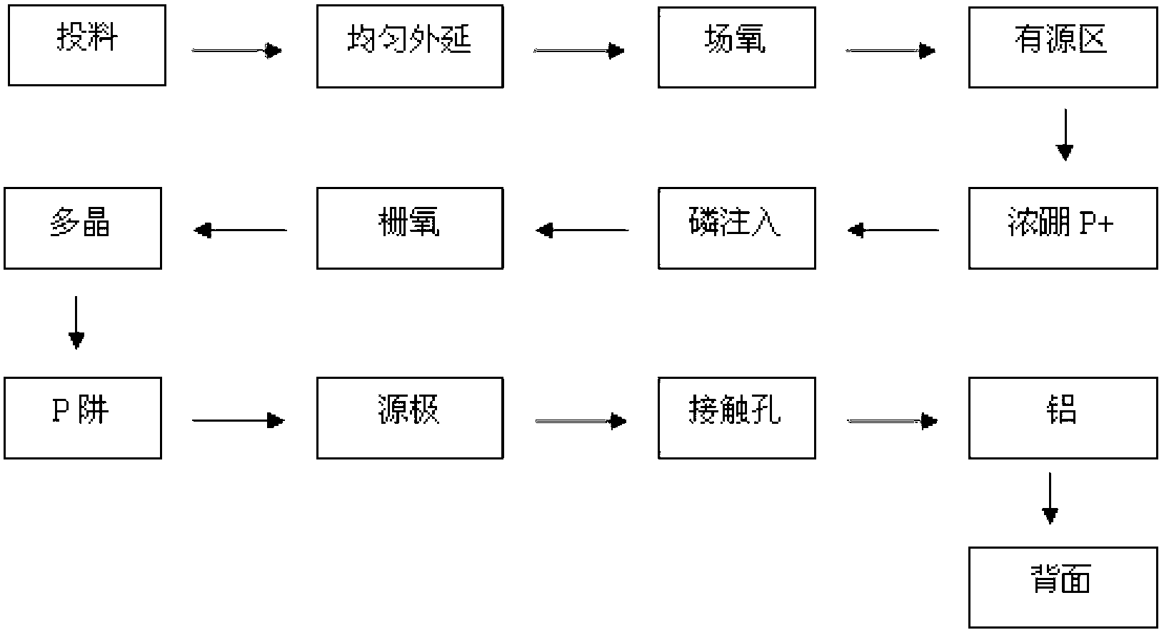

Image

  • Process for manufacturing series of intermediate-voltage N-type vertical conduction double-diffused metal oxide semiconductor transistors by using composite epitaxy
  • Process for manufacturing series of intermediate-voltage N-type vertical conduction double-diffused metal oxide semiconductor transistors by using composite epitaxy
  • Process for manufacturing series of intermediate-voltage N-type vertical conduction double-diffused metal oxide semiconductor transistors by using composite epitaxy

Examples


Embodiment Construction

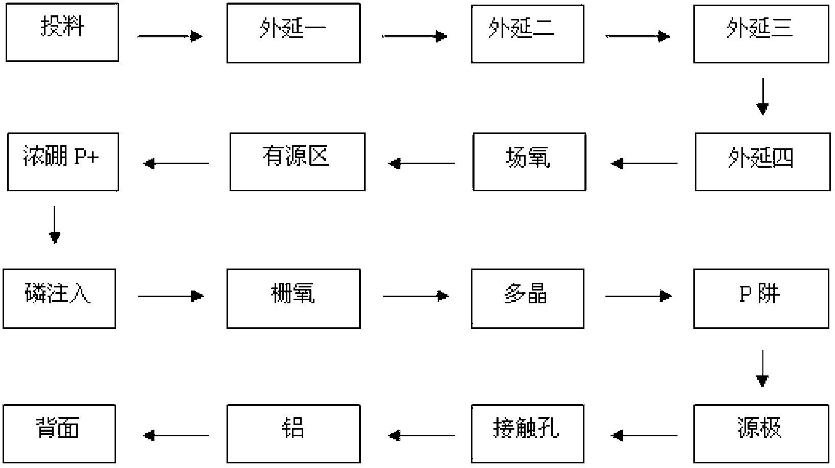
[0046] Such as figure 2 Shown is a composite epitaxy process for manufacturing medium-voltage series vertical double-diffused field effect transistors. The specific implementation method is as follows:

[0047] 1) Feeding: arsenic-doped or antimony-doped substrate silicon wafer material, with a resistivity of 0.03ohm.cm or below.

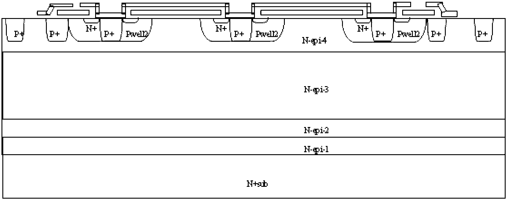
[0048] 2) The first step of epitaxy: grow N-type epitaxy with a thickness of 4um and a resistivity of 1 ohm.cm. It is used to form a high-concentration transition zone with a high-concentration substrate. On-resistance can be reduced.

[0049] 3) The second step of epitaxy: grow N-type epitaxy with a thickness of 4um and a resistivity of 10 ohm.cm. It is used to epitaxially form a medium-concentration transition region with the high-concentration first part. On-resistance can also be reduced.

[0050] 4) The third step of epitaxy: grow N-type epitaxy with a thickness of 42um and a resistivity of 18 ohm.cm. Provide a withstand voltage layer fo...


PUM


Abstract

The invention discloses a process for manufacturing series of intermediate-voltage N-type vertical conduction double-diffused metal oxide semiconductor (VDMOS) transistors by using composite epitaxy. The process comprises the steps of: batch feeding, first-step epitaxy, second-step epitaxy, third-step epitaxy, fourth-step epitaxy, field oxidation, etching of an active area, high-concentration boron injection and junction depth increasing, phosphorus injection and junction depth increasing, gate oxidation, polycrystalline silicon gate deposition and doping, PWELL boron injection and junction depth increasing, source N+ arsenic injection and junction depth increasing, contact hole etching, aluminum evaporation and corrosion, back thinning evaporation and the like. By a process platform, any additional procedure and operation is avoided, and on-resistance can be lowered by 10 percent on the basis of ensuring withstand voltage; by the VDMOS transistor manufactured by the process, a high-current intense-electric field effect can be effectively suppressed, and the safety working area of a device is enlarged to a certain extent; and the on-resistance is lowered, so that power consumption is greatly reduced, energy sources are saved, and the reliability of a circuit is greatly improved.

Description

technical field [0001] The invention relates to a VDMOS process method for manufacturing medium-voltage resistant N-type series (withstand voltage 600V, conduction current ranging from 1 ampere to 15 amperes), and belongs to the technical field of semiconductor manufacturing. Background technique [0002] The full name of VDMOS is Vertical conduction double-diffused metal oxide semiconductor, that is, vertical double-diffused metal oxide semiconductor field effect transistor, which was proposed by H.W.Collins et al. in 1979. [0003] After more than 30 years of development, VDMOS transistors have made great progress. With a series of advantages such as high input impedance, low on-resistance and high switching speed, it has been widely used in switching regulated power supplies, high-frequency heating, computer interface circuits and power amplifiers. To be sure, with the further deepening of people's understanding of energy saving and emission reduction, the switching powe...

Claims


Application Information

Patent Timeline
Patent Type & Authority Applications(China)
IPC IPC(8): H01L21/336
Inventor 聂卫东沈克强易法友
Owner WUXI CRYSTAL SOURCE MICROELECTRONICS CO LTD
Learn More