

Oxide thin-film, thin-film transistor and preparation method thereof
A technology of oxide thin film and thin film transistor, which is applied in the direction of transistor, semiconductor/solid-state device manufacturing, semiconductor device, etc., can solve the problems of thin film transistor threshold voltage switch ratio influence, weak suppression ability, etc., to improve reliability and electrical characteristics , enhance the inhibitory ability, increase the effect of crystallization temperature
- Summary
- Abstract
- Description
- Claims
- Application Information
AI Technical Summary
Problems solved by technology
Method used
Image

Examples
Embodiment 1
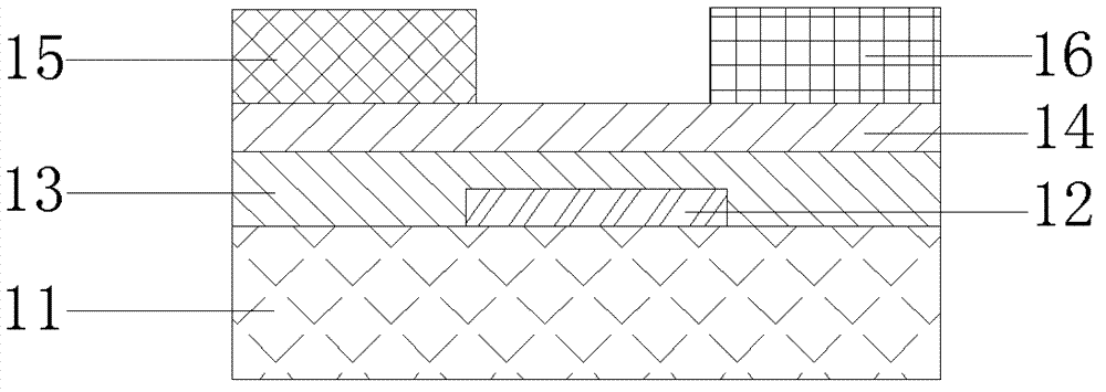
[0057] figure 1It is a schematic structural diagram of a bottom-gate staggered thin film transistor (TFT with inverted staggered structure) described in the first embodiment of the present invention, as shown in figure 1 As shown, the bottom gate staggered thin film transistor includes: a substrate 11 , a gate electrode 12 , a gate insulating layer 13 , an oxide thin film channel layer 14 , a source region 15 and a drain region 16 .
[0058] The gate electrode 12 is disposed above the substrate 11 . The substrate 11 can be made of silicon, glass or plastic.
[0059] The gate insulating layer 13 is disposed above the gate electrode 12 and the portion of the substrate 11 not covered by the gate electrode 12 .
[0060] The oxide film channel layer 14 is disposed above the gate insulating layer 13 . The general chemical formula of the oxide thin film used in the oxide thin film channel layer 14 is In-X-Zn-O, wherein X is Si, Ge, La or Y element. The oxide film is also doped wi...
Embodiment 2
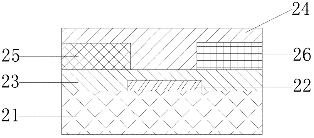
[0072] image 3 It is a schematic structural diagram of a bottom-gate coplanar thin film transistor (TFT with inverted staggered structure) described in the second embodiment of the present invention, as shown in image 3 As shown, the bottom-gate coplanar thin film transistor includes: a substrate 21 , a gate electrode 22 , a gate insulating layer 23 , an oxide film channel layer 24 , a source region 25 and a drain region 26 . The materials used for each component in the bottom-gate coplanar thin film transistor are the same as those in the bottom-gate staggered thin film transistor described in Embodiment 1, the difference lies in that the structure of each component is as follows:
[0073] The gate electrode 22 is disposed above the substrate 21;
[0074] The gate insulating layer 23 is disposed above the gate electrode 22 and the portion of the substrate 21 not covered by the gate electrode 22;
[0075] The source region 25 is disposed on one side above the gate insulati...
Embodiment 3
[0080] Figure 4 It is a schematic structural diagram of a top gate staggered thin film transistor (TFT with top gate staggered structure) described in the third embodiment of the present invention, as shown in Figure 4 As shown, the top gate staggered thin film transistor includes: a substrate 31 , a gate electrode 32 , a gate insulating layer 33 , an oxide thin film channel layer 34 , a source region 35 and a drain region 36 . The components in the top-gate staggered thin film transistor are made of the same materials as those in the bottom-gate staggered thin film transistor in Embodiment 1, the difference lies in the structure of each component is as follows:
[0081] The source region 35 is disposed on one side above the substrate 31;
[0082] The drain region 36 is disposed on the other side above the substrate 31;
[0083] The oxide film channel layer 34 is disposed above the source region 35 and the drain region 36 and the portion of the substrate 31 not covered by ...
PUM
| Property | Measurement | Unit |
|---|---|---|
| Mobility | aaaaa | aaaaa |
Abstract
Description
Claims
Application Information