

Electromagnetic energy harvester with flexible substrate and method for preparing electromagnetic energy harvester
An energy harvester and flexible substrate technology, applied in electromechanical devices, electrical components, manufacturing microstructure devices, etc., can solve the problems of difficult adhesion of permanent magnets and low output energy, and achieve small size, high output power, and good biocompatibility. sexual effect
- Summary
- Abstract
- Description
- Claims
- Application Information
AI Technical Summary
Problems solved by technology
Method used
Image

Examples
Embodiment 1
[0047] Embodiment 1: comprise the steps:
[0048] (1) Preparation of Parylene film
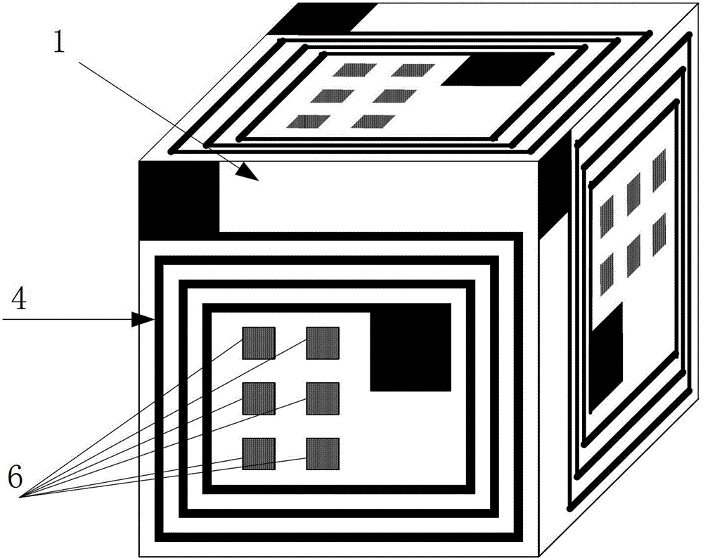
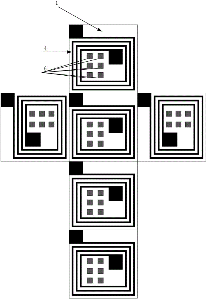
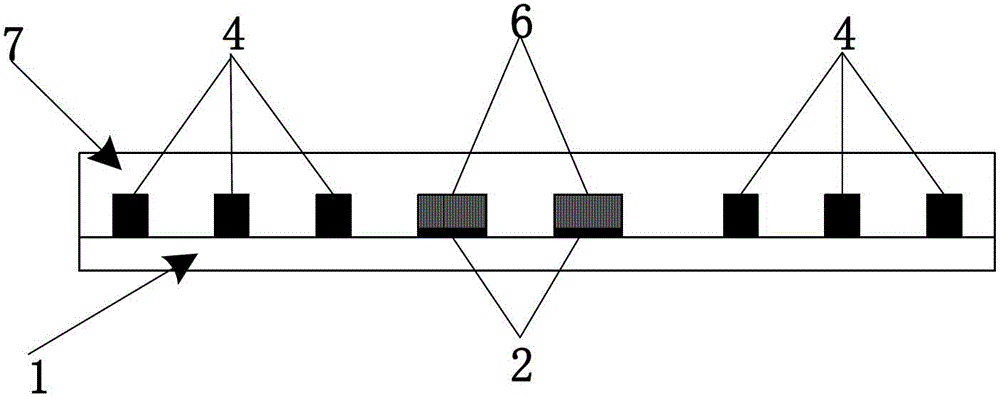
[0049] Silicon wafer cleaning and other treatment processes, such as Figure 5 (a) shown. A 10 μm thick Parylene film was prepared on a silicon wafer by vacuum deposition (ie evaporation and condensation method). The solid Parylene raw material is sublimated into a gaseous state at 120°C in vacuum, and the gaseous raw material is cracked into reactive monomers at 650°C. The gaseous monomers are deposited and polymerized at room temperature to form a Parylene film, such as Figure 5 (b) shown. In addition to silicon wafers, other substrates such as glass can also be used.
[0050] (2) Sputtering Ti / Cu seed layer
[0051] The Ti / Cu seed layer was prepared by vacuum sputtering. Sputtering for 1 hour under the condition of 50W power in a vacuum environment can obtain a Ti / Cu seed layer with a total thickness of 200nm, such as Figure 5 (c) shown.
[0052] (3) Cu coil preparation
[0053] ...
Embodiment 2
[0062] Embodiment 2: comprise the steps:
[0063] (1) Preparation of Parylene film
[0064] Carry out cleaning and other treatment processes on silicon wafers. A 10 μm Parylene film was prepared on a silicon wafer by vacuum deposition. The solid raw material is sublimated into a gaseous state at 120°C in vacuum, and the gaseous raw material is cracked into reactive monomers at 650°C, and the gaseous monomers are deposited and polymerized at room temperature to form a Parylene film.
[0065] (2) Sputtering Ti / Cu seed layer
[0066] A 200 nm Ti / Cu seed layer was prepared by vacuum sputtering. A Ti / Cu seed layer with a total thickness of 200 nm can be obtained by sputtering for 30 min under the condition of 100 W power in a vacuum environment.
[0067] (3) Cu coil preparation
[0068] Spin-coat 10μm thick positive resist AZ P4620 on the Ti / Cu seed layer, expose for 180s, develop for 100s, and then electroplate Cu coils. Electroplating conditions: the current density is 10mA...
Embodiment 3
[0077] Embodiment 3: comprise the steps:
[0078](1) Preparation of Parylene film
[0079] Carry out cleaning and other treatment processes on silicon wafers. A 10 μm Parylene film was prepared on a silicon wafer by vacuum deposition. The solid raw material is sublimated into a gaseous state at 120°C in vacuum, and the gaseous raw material is cracked into reactive monomers at 650°C, and the gaseous monomers are deposited and polymerized at room temperature to form a Parylene film.
[0080] (2) Sputtering Ti / Cu seed layer
[0081] A 200 nm Ti / Cu seed layer was prepared by vacuum sputtering. A Ti / Cu seed layer with a total thickness of 200 nm can be obtained by sputtering for 1 hour under the condition of a power of 50 W in a vacuum environment.
[0082] (3) Cu coil preparation
[0083] Spin-coat 10μm thick positive resist AZ P4620 on the Ti / Cu seed layer, expose for 180s, develop for 100s, and then electroplate Cu coils. Electroplating conditions: the current density is 5...
PUM
| Property | Measurement | Unit |
|---|---|---|
| thickness | aaaaa | aaaaa |
| thickness | aaaaa | aaaaa |
| thickness | aaaaa | aaaaa |
Abstract
Description
Claims
Application Information