Three-strained fully planar SOI (silicon on insulator) BiCMOS (bipolar complementary metal oxide semiconductor) integrated device and preparation method

An integrated device, full-plane technology, used in semiconductor/solid-state device manufacturing, semiconductor devices, electric solid-state devices, etc., can solve the problems of low mechanical strength, high cost, incompatibility with wide application and development, etc.

Inactive Publication Date: 2012-10-17
XIDIAN UNIV
View PDF2 Cites 0 Cited by
  • Summary
  • Abstract
  • Description
  • Claims
  • Application Information

AI Technical Summary

Problems solved by technology

Although GaAs and InP-based compound devices have superior frequency characteristics, their preparation process is more complicated than Si process, high cost, difficult to prepare large-diameter single

Method used


Image

  • Three-strained fully planar SOI (silicon on insulator) BiCMOS (bipolar complementary metal oxide semiconductor) integrated device and preparation method

Examples


Embodiment 1

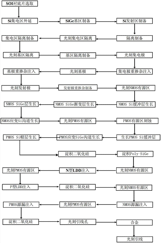
[0108] Embodiment 1: Preparation of conductive channel 22nm three-strain, full-plane SOI BiCMOS integrated device and circuit, the specific steps are as follows:

[0109] Step 1, epitaxial growth.

[0110] (1a) Select the SOI substrate, the support material of the lower layer of the substrate is Si, and the middle layer is SiO 2 , with a thickness of 150nm, and the upper material is doped with a concentration of 1×10 16 cm -3 N-type Si with a thickness of 100nm;

[0111] (1b) Using chemical vapor deposition (CVD), grow a layer of N-type epitaxial Si layer with a thickness of 50nm on the upper Si material at 600°C, as the collector region, and the doping concentration of this layer is 1× 10 16 cm -3 ;

[0112] (1c) Using chemical vapor deposition (CVD), grow a SiGe layer with a thickness of 20nm on the substrate at 600°C. As the base region, the Ge composition of this layer is 15%, and the doping concentration is 5×10 18 cm -3 ;

[0113] (1d) Using the method of chemi...

Embodiment 2

[0167] Embodiment 2: Prepare conductive channel 30nm three-strain, full-plane SOI BiCMOS integrated device and circuit, the specific steps are as follows:

[0168] Step 1, epitaxial growth.

[0169] (1a) Select the SOI substrate, the support material of the lower layer of the substrate is Si, and the middle layer is SiO 2 , with a thickness of 300nm, and the upper material is doped with a concentration of 5×10 16 cm -3 N-type Si with a thickness of 120nm;

[0170] (1b) Using chemical vapor deposition (CVD), grow an N-type epitaxial Si layer with a thickness of 80nm on the upper Si material at 700°C as the collector region, and the doping concentration of this layer is 5× 10 16 cm -3 ;

[0171] (1c) Using chemical vapor deposition (CVD), grow a layer of SiGe layer with a thickness of 40nm on the substrate at 700°C. As the base region, the Ge composition of this layer is 20%, and the doping concentration is 1×10 19 cm -3 ;

[0172] (1d) Using the method of chemical vap...

Embodiment 3

[0226] Embodiment 3: Prepare a three-strain, full-plane SOI BiCMOS integrated device and circuit with a 45nm conductive channel, and the specific steps are as follows:

[0227]Step 1, epitaxial growth.

[0228] (1a) Select the SOI substrate, the support material of the lower layer of the substrate is Si, and the middle layer is SiO 2 , with a thickness of 400nm, and the upper material is doped with a concentration of 1×10 17 cm -3 N-type Si with a thickness of 150nm;

[0229] (1b) Using the method of chemical vapor deposition (CVD), grow a layer of N-type epitaxial Si layer with a thickness of 100nm on the upper layer of Si material at 750°C, as the collector region, and the doping concentration of this layer is 1× 10 17 cm -3 ;

[0230] (1c) Using chemical vapor deposition (CVD), grow a layer of SiGe layer with a thickness of 60nm on the substrate at 750°C. As the base region, the Ge composition of this layer is 25%, and the doping concentration is 5×10 19 cm -3 ;

...


PUM

PropertyMeasurementUnit
Thicknessaaaaaaaaaa
Thicknessaaaaaaaaaa
Thicknessaaaaaaaaaa

Abstract

The invention discloses a three-strained fully planar SOI BiCMOS integrated device and a preparation method. The preparation method comprises continuously growing an N-Si layer, a P-SiGe layer and an N-Si layer on an SOI substrate, preparing deep trench isolation, etching a collector region, a base region and a shallow trench isolation region by lithography respectively, carrying out ion implantation, forming a collector, base and emitter contact region, and finally forming a SiGe HBT (heterojunction bipolar transistor) device; etching a trench in the active region of an NMOS (n-type metal oxide semiconductor) by lithography, growing four material layers in the trench, and preparing a gate dielectric layer and gate polysilicon on the active region of the NMOS device to obtain the NMOS device; etching a trench in the active region of a PMOS (p-type metal oxide semiconductor) by lithography, growing three material layers in the trench, and preparing a drain and a gate on the active region of the PMOS device to obtain the PMOS device; and etching leads by lithography to obtain the three-strained fully planar SOI BiCMOS integrated device and circuit. The preparation method provided by the invention adopts the self-alignment process, and fully utilizes the characteristics that the electron mobility of a tensile strained Si material is higher than that of a bulk Si material and that the hole mobility of a compressive strained SiGe material is higher than that of the bulk Si material so as to prepare the performance-enhanced three-strained fully planar SOI BiCMOS integrated circuit.

Description

technical field [0001] The invention belongs to the technical field of semiconductor integrated circuits, and in particular relates to a three-strain full-plane SOI BiCMOS integrated device and a preparation method. Background technique [0002] Integrated circuits are the cornerstone and core of the economic development of an information society. Just as the American engineering and technology circle recently named the fifth electronic technology among the 20 greatest engineering and technological achievements in the world in the 20th century, "from vacuum tubes to semiconductors and integrated circuits, they have become the cornerstone of intelligent work in various industries today." Integrated circuits. It is one of the typical products that can best reflect the characteristics of knowledge economy. At present, the electronic information industry based on integrated circuits has become the world's largest industry. With the development of integrated circuit technology,...

Claims


Application Information

Patent Timeline
IPC IPC(8): H01L27/12H01L21/84
Inventor 张鹤鸣吕懿宣荣喜王斌胡辉勇周春宇宋建军郝跃
Owner XIDIAN UNIV
Why Eureka
Try Eureka