
Heterojunction solar cell structure and manufacturing method thereof

A technology for solar cells and fabrication methods, which are applied to circuits, photovoltaic power generation, electrical components, etc., can solve the problems of increasing the series resistance of heterojunction cells, low photoelectric conversion efficiency, and high TCO resistivity, so as to improve battery efficiency and reduce battery Resistivity, the effect of improving light transmittance

Inactive Publication Date: 2012-10-24
TRINA SOLAR CO LTD
View PDF3 Cites 5 Cited by
  • Summary
  • Abstract
  • Description
  • Claims
  • Application Information

AI Technical Summary

Problems solved by technology

[0002] Although the existing heterojunction solar cells have a multi-layer structure, they have low light absorption rate and low photoelectric conversion efficiency, and the high TCO resistivity is easy to increase the series resistance of heterojunction cells, and it is easy to overlap due to magnetron sputtering. Amorphous silicon in the layer causes damage, increasing the defectivity of the cell
Affect battery efficiency

Method used


Image

  • Heterojunction solar cell structure and manufacturing method thereof
  • Heterojunction solar cell structure and manufacturing method thereof

Examples


Embodiment Construction

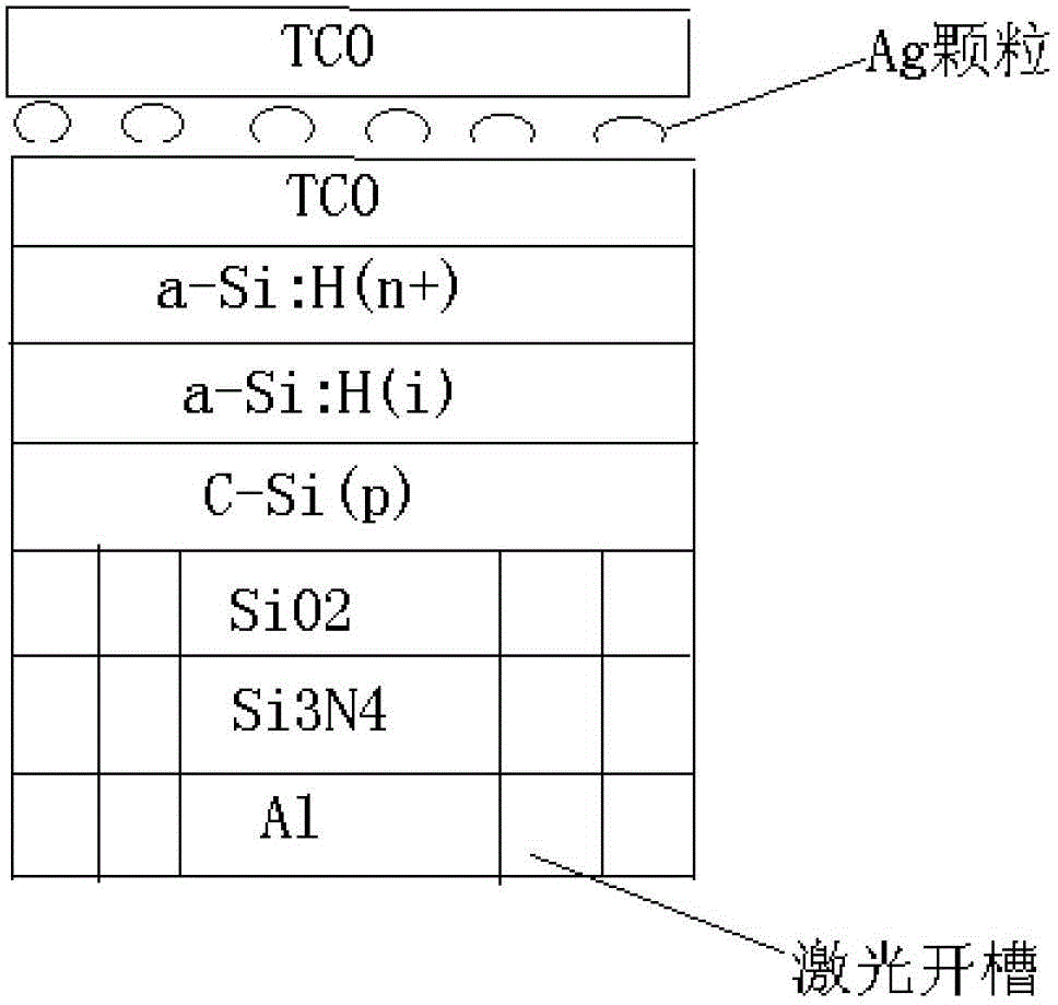
[0016] A heterojunction solar cell structure, comprising a silicon wafer substrate, an amorphous silicon layer for forming a heterojunction on the light-receiving surface of the silicon wafer substrate, a transparent conductive film on the amorphous silicon layer, and a transparent conductive film on the transparent conductive film Make the gate line, the transparent conductive film includes the bottom TCO layer, the middle Ag layer and the surface TCO layer, the bottom TCO layer is 10-20nm thick, the middle Ag layer is 10-15nm, and the surface TCO layer is 80-100nm thick .

[0017] Such as figure 1 As shown, the silicon wafer substrate is P-type, and the amorphous silicon layer on the P-type silicon wafer substrate includes an intrinsic amorphous silicon layer and an n+ amorphous silicon layer on the intrinsic amorphous silicon layer.

[0018] A silicon dioxide layer, a silicon nitride layer and an aluminum layer are sequentially arranged on the backlight surface of the sili...


PUM

PropertyMeasurementUnit
Thicknessaaaaaaaaaa
Thicknessaaaaaaaaaa

Abstract

The invention relates to a heterojunction solar cell structure and a manufacturing method thereof. A transparent conductive oxide (TCO) / silver (Ag) / TCO transparent conductive film is manufactured on an amorphous silicon layer to form the cell structure. The manufacturing method is that a silicon dioxide layer, a silicon nitride layer and an aluminum layer are sequentially manufactured on the back of a P-type silicon wafer substrate, laser sintering is used for punching the back of the silicon wafer substrate, and then annealing is performed at a pure nitrogen atmosphere at the temperature between 300 DEG C and 400 DEG C; a silicon wafer is turned, an intrinsic amorphous silicon layer is deposited on the front of the silicon wafer, then an n<+> amorphous silicon layer is deposited, a TCO layer, an Ag layer and a TCO layer are deposited by magnetron sputtering to form the TCO / Ag / TCO transparent conductive film, and then the annealing is performed for 10-30 minutes at a mixed atmosphere of nitrogen and hydrogen with the temperature between 320 DEG C and 450 DEG C. The heterojunction solar cell structure and the manufacturing method thereof have the advantages that the Ag layer is added to the TCO layer so that the resistivity of the cell can be reduced, the series resistance is reduced, and the short-circuit current is increased; the silicon dioxide layer is added to improve back passivation and reduce recombination velocity; and the annealing is performed after the transparent conducting film is formed by depositing so that the light transmittance can be improved and the resistance can be reduced.

Description

technical field [0001] The invention relates to a heterojunction solar cell structure and a manufacturing method thereof. Background technique [0002] Although the existing heterojunction solar cells have a multi-layer structure, they have low light absorption rate and low photoelectric conversion efficiency, and the high TCO resistivity is easy to increase the series resistance of heterojunction cells, and it is easy to overlap due to magnetron sputtering. The amorphous silicon in the layer causes damage, increasing the defects of the cell. affect battery efficiency. Contents of the invention [0003] The technical problem to be solved by the present invention is to provide a heterojunction solar cell structure and a manufacturing method thereof, so as to improve cell efficiency. [0004] The technical solution adopted by the present invention to solve the technical problem is: a heterojunction solar cell structure, including a silicon substrate, and an amorphous silic...

Claims


Application Information

Patent Timeline
IPC IPC(8): H01L31/0224H01L31/0216H01L31/077H01L31/20
CPCY02E10/50Y02E10/547Y02P70/50
Inventor 董科研
Owner TRINA SOLAR CO LTD
Learn More