
Preparation method of low-stress gallium nitride epitaxial layer

A gallium nitride and epitaxial layer technology, applied in the field of optoelectronics, can solve the problems of reducing the stress of gallium nitride, unfavorable production process stability and repeatability, etc.

Active Publication Date: 2012-10-31
吴江市民福电缆附件厂
View PDF8 Cites 11 Cited by
  • Summary
  • Abstract
  • Description
  • Claims
  • Application Information

AI Technical Summary

Problems solved by technology

The above-mentioned patents improve the stress by adding a special stress relief structure to the epitaxial structure, but these epitaxial structures can only reduce the influence of the stress on the active region after the GaN epitaxial layer is grown, but cannot fundamentally Reducing Stress During Gallium Nitride Growth
Moreover, adding these complex structures in the light-emitting diode structure is not conducive to the stability and repeatability of the production process.

Method used


Image

  • Preparation method of low-stress gallium nitride epitaxial layer
  • Preparation method of low-stress gallium nitride epitaxial layer
  • Preparation method of low-stress gallium nitride epitaxial layer

Examples


Embodiment Construction

[0011] Technical scheme of the present invention is as follows:

[0012] A method for preparing a low-stress gallium nitride epitaxial layer, the steps are as follows:

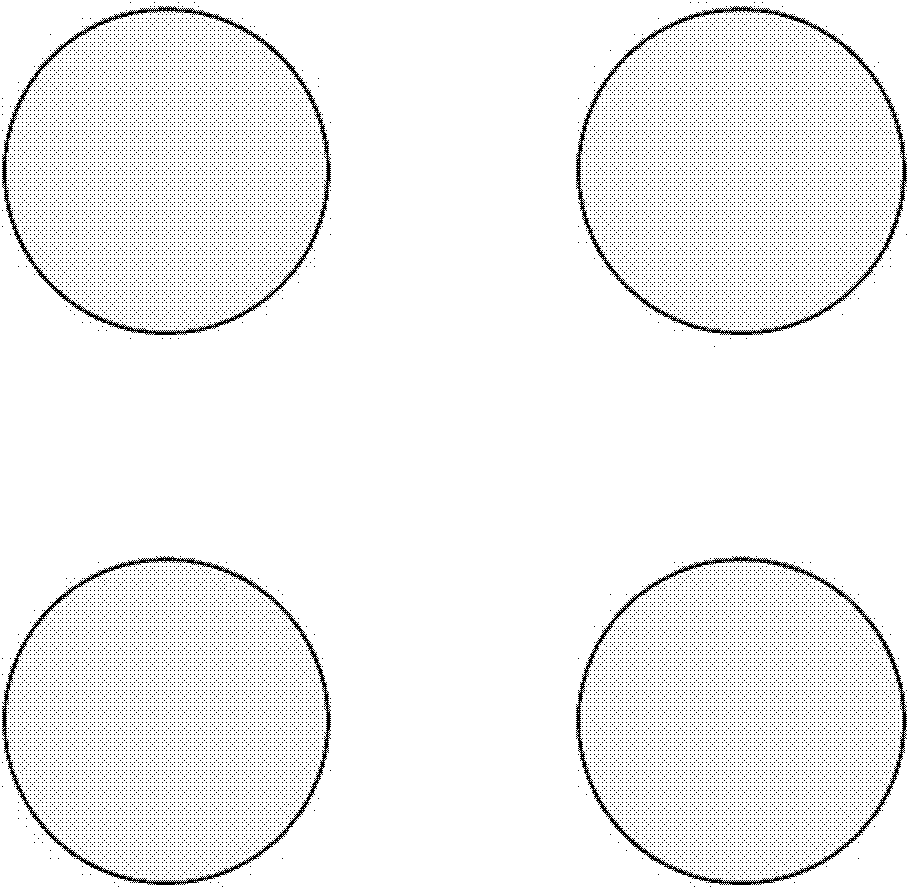
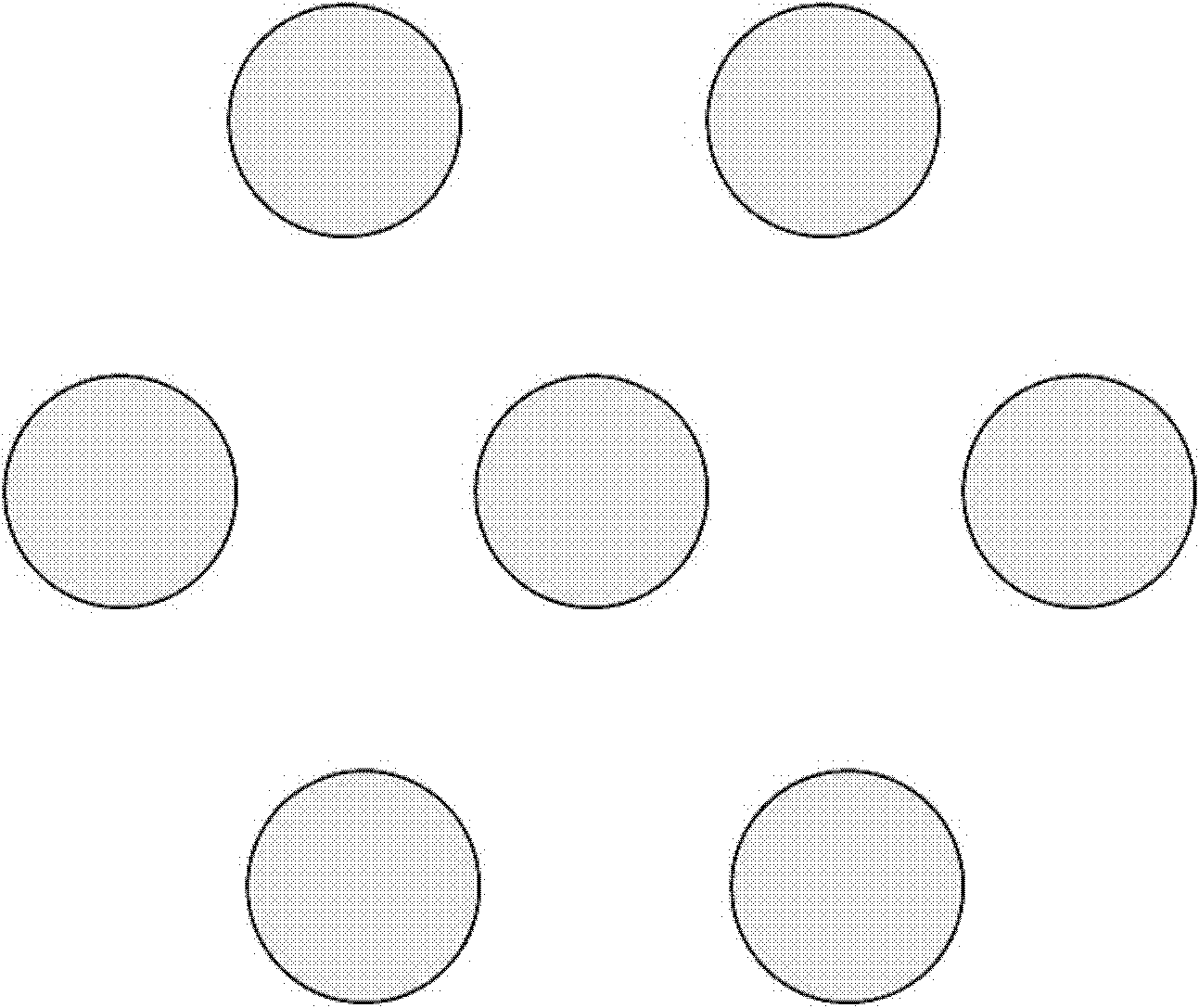
[0013] 1) Etching the front or back of the substrate by dry etching, the etching depth is 1 μm-100 μm, the etching pattern is square or circular, and the size range of its side length or diameter is 0.2mm-5mm, The spacing between the patterns is 1 μm-10 μm.

[0014] 2) Corroding the etched substrate with sulfuric acid or a mixed solution of sulfuric acid / phosphoric acid, the etching time is 1 min-30 min at normal temperature, or 1 min-10 min at 50-200° C. The purpose of this step is to remove the etch marks and impurities produced by the etching described in step 1).

[0015] 3) Wash the substrate treated in step 2) with deionized water, and spin dry. Drying or air drying can also be used here, but in order to avoid water marks, spin drying is preferred.

[0016] 4) On the front side of the substrate treat...


PUM

PropertyMeasurementUnit
depthaaaaaaaaaa
depthaaaaaaaaaa
thicknessaaaaaaaaaa

Abstract

The invention relates to a preparation method of a low-stress gallium nitride epitaxial layer. The preparation method includes: etching square or round patterns on the front or the back of a substrate; corroding the etched substrate layer with sulfuric acid or sulfuric acid / phosphoric acid mixed solution, cleaning with deionized water, and growing the gallium nitride epitaxial layer on the processed front of the substrate by an MOCVD (metal organic chemical vapor deposition) method; wherein etching depth of the patterns is 1-100 micrometers, and space between each two patterns is 1-10 micrometers. By the preparation method, low stress is borne by the gallium nitride epitaxial layer when the gallium nitride epitaxial layer grows on the processed substrate, production process is simplified, production stability is improved, piezoelectric polarization of active area of a light-emitting diode is avoided, and light-emitting efficiency of the light-emitting diode is improved. The light-emitting efficiency of the light-emitting diode made by the low-stress gallium nitride epitaxial layer is improved by 10%.

Description

technical field [0001] The invention relates to a method for preparing a low-stress gallium nitride epitaxial layer, belonging to the field of optoelectronic technology. Background technique [0002] In recent years, semiconductor light-emitting diodes have received widespread attention, because they have the advantages of small size, high efficiency, and long life. The rapid development of gallium nitride semiconductor materials has enabled the commercialization of high-brightness light-emitting diodes from green light to near-ultraviolet products. At present, light-emitting diodes ranging from ordinary green to ultraviolet are widely used in traffic lights, full-color displays, backlight panels of LCD screens, automotive instruments and interior lights, etc. In recent years, ultraviolet light-emitting diodes have entered the market and are mainly used for the detection of biological particles (such as the detection of bacterial spores with an absorption range of 260-340nm...

Claims


Application Information

Patent Timeline
Patent Type & Authority Applications(China)
IPC IPC(8): H01L33/00
Inventor 曲爽徐现刚邵慧慧王成新李树强
Owner 吴江市民福电缆附件厂
Learn More