Method for producing indium gallium zinc oxide semiconductor thin film by using sol-gel method

A technology of indium gallium zinc oxide and sol-gel method is applied in the field of preparing oxide semiconductor thin films by sol-gel method, which can solve the problems of high cost, low price of precursors, explosion and the like

Inactive Publication Date: 2012-11-07
FUDAN UNIV
View PDF3 Cites 25 Cited by
  • Summary
  • Abstract
  • Description
  • Claims
  • Application Information

AI Technical Summary

Problems solved by technology

However, because the precursors with low decomposition temperatures are very unstable, there is a danger of explosion if there is a slight vibration, and currently there are too few precursors with low decompositio

Method used


Image

  • Method for producing indium gallium zinc oxide semiconductor thin film by using sol-gel method
  • Method for producing indium gallium zinc oxide semiconductor thin film by using sol-gel method
  • Method for producing indium gallium zinc oxide semiconductor thin film by using sol-gel method

Examples


Embodiment Construction

[0023] The specific implementation steps of the present invention are specifically set forth below by specific examples:

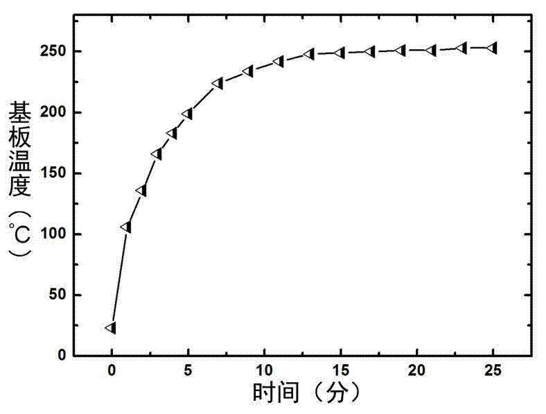
[0024] With ethylene glycol monomethyl ether as solvent and monoethanolamine as stabilizer, In(NO 3 ) 3 4.5H 2 O, Ga(NO 3 ) 3 4.5H 2 O, Zn(C 2 h 3 o 2 ) 2 ·5H 2 O was dissolved in it, and left to stand for 48 hours after ultrasonic oscillation for 1 hour to form a clear and stable precursor solution, wherein the volume ratio of ethylene glycol monomethyl ether to monoethanolamine was 10:1, and In ions, Ga ions, and Zn ions in the solution The molar ratio of Zn ions is 2:1:1, and the molar concentration of Zn ions is 0.3M; the precursor solution is spin-coated on a common glass substrate, and irradiated under an infrared heating lamp to obtain a 40 nm IGZO semiconductor film, and the spin-coating speed is 5500 rpm, the power of the infrared heating lamp is 275W, and the distance between the light source and the film is 10 mm during irradiation (th...


PUM


Abstract

The invention belongs to the technical field of preparation of semiconductor thin films, and particularly relates to a low-temperature treatment method for producing an indium gallium zinc oxide (IGZO) semiconductor thin film by using a sol-gel method. The method comprises the following steps of: dissolving In(NO3)3.4*5H2O, Ga(NO3)3.4*5H2O and Zn(C2H3O2)2*5H2O into ethylene glycol monomethyl ether serving as a solvent and monoethanolamine serving as a stabilization agent to form a clear stable precursor solution; and coating the precursor solution on a glass substrate in a rotatable manner, and irradiating by using an infrared heating lamp to obtain the flat and transparent IGZO semiconductor thin film. Compared with the conventional method for preparing the IGZO thin film through annealing of a heat plate by using the sol-gel method, the method has the advantages that the IGZO thin film irradiated by the infrared heating lamp is relatively high in semiconductor and optical properties, and the process temperature is relatively low and lower than 250 DEG C; the IGZO thin film is used as a thin film transistor with a trench layer material; the switch current ratio is more than 5*10<6>; the saturated migration rate is more than 1.8 cm<2>/Vs; and the subthreshold amplitude is less than 2.2 V/dec.

Description

technical field [0001] The invention belongs to the technical field of semiconductor thin film preparation, and in particular relates to a method for preparing an oxide semiconductor thin film by a sol-gel method. Background technique [0002] A thin film transistor (Thin Film Transistor: TFT) is a field effect transistor (Field Effect Transistor: FET), which consists of a semiconductor active layer, namely the channel layer, a dielectric layer, namely the insulating layer, a gate electrode, a source electrode and a drain electrode. Field-effect transistors are widely used in various electronic circuits due to their small size, light weight, long life, and low power consumption. In the 1960s, based on the actual demand for low-cost, large-array displays, research on TFTs was widely developed. In 1988, when the first 14-inch Active-Matrix (Active-Matrix: AM) Thin Film Transistor Liquid Crystal Displays (Thin Film Transistor Liquid Crystal Displays: TFT-LCD) appeared, people ...

Claims


Application Information

Patent Timeline
IPC IPC(8): H01L21/02
Inventor 浦海峰张群
Owner FUDAN UNIV
Why Eureka
Try Eureka