Polycrystalline silicon ingot, manufacturing method thereof and solar cell

A technology of polycrystalline silicon ingots and manufacturing methods, which is applied in the direction of polycrystalline material growth, chemical instruments and methods, circuits, etc., can solve the problems of low photoelectric conversion efficiency, low minority carrier lifetime, and small crystal grains, and achieve high photoelectric conversion efficiency and reduce The effect of oxygen impurity content and low attenuation coefficient

Inactive Publication Date: 2012-11-28
ZHEJIANG YUHUI SOLAR ENERGY SOURCE
View PDF13 Cites 9 Cited by
  • Summary
  • Abstract
  • Description
  • Claims
  • Application Information

AI Technical Summary

Problems solved by technology

Compared with monocrystalline silicon ingots, there are more defects in polycrystalline silicon ingots, the grains are small, and there are more grain boundaries and dislocations between conventional polycrystalline silicon grains, resulting in rapid recombination of charge carriers, resulting in low minority carrier lifetime. , and, because the orientation between crystal grains is random, it is difficult to texture the surface of the wafer well, so that the photoelectric conversion efficiency of conventional polycrystalline silicon solar cells is lower than that of monocrystalline silicon solar cells, but the oxygen content in polycrystalline silicon ingots It can be controlled at a good level, so that the attenuation coefficient of polycrystalline silicon solar cells is low

Method used


Image

  • Polycrystalline silicon ingot, manufacturing method thereof and solar cell
  • Polycrystalline silicon ingot, manufacturing method thereof and solar cell
  • Polycrystalline silicon ingot, manufacturing method thereof and solar cell

Examples


Embodiment 1

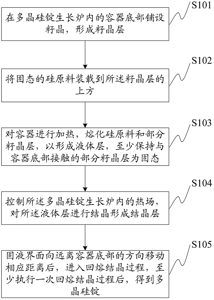
[0049] Based on the above research, an embodiment of the present invention provides a method for manufacturing a polycrystalline silicon ingot, the flow chart of the method is as follows figure 1 shown, including the following steps:

[0050] Step S101: laying seed crystals on the bottom of the container in the polycrystalline silicon ingot growth furnace to form a seed crystal layer;

[0051] Wherein, the seed crystal is single crystal silicon with a fixed crystallographic orientation, and the seed layer includes at least one single crystal silicon layer with crystallographic orientation. Preferably, the seed crystals in this embodiment are (100), ( 110) or (111) oriented single crystal silicon.

[0052] Specifically, in this embodiment, the seed layer includes at least one single-crystal silicon layer with crystallographic orientation. In other words, all the seed layers can be selected to have single-crystal silicon with the same crystallographic orientation. ) oriented s...

Embodiment 2

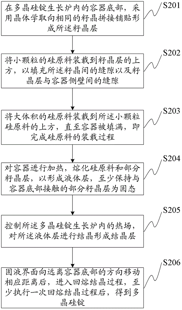
[0077] The flow chart of the casting method of the polycrystalline silicon ingot disclosed in this embodiment is as follows: image 3 As shown, different from the previous embodiment, in this embodiment, the process of loading silicon raw materials is embodied, and the method includes the following steps:

[0078] Step S201: at the bottom of the container in the polycrystalline silicon ingot growth furnace, the seed crystal layer is formed by splicing and tiling seed crystals with the same crystallographic orientation, and the seed crystal layer is substantially parallel to the bottom of the container;

[0079] In this embodiment, the seed layer is preferably formed by paving (100)-oriented single crystal silicon. Preferably, the area of ​​the seed layer accounts for the percentage of the bottom area of ​​the container, that is, the area of ​​the seed layer is The percentage of the area occupying the bottom area of ​​the container is 50%-99%, more preferably, the area of ​​the...

Embodiment 3

[0087] This embodiment discloses the polycrystalline silicon ingot manufactured by the method of each of the above embodiments, and the solar wafer and the solar cell manufactured by using the manufactured polycrystalline silicon ingot.

[0088] Wherein, the polycrystalline silicon ingot contains continuous large-sized single crystal silicon regions with consistent crystallographic orientations, and after cutting off the impurity-enriched layers at both ends of the polycrystalline silicon ingot, other main regions are cut to obtain solar wafers, and the wafers are used Making a solar cell, the solar cell comprising:

[0089] a wafer having contiguous large-scale regions of single crystal silicon of uniform crystallographic orientation;

[0090] P-N junctions in the wafer;

[0091] conductive contacts on the wafer.

[0092] In addition, it also includes an anti-reflection film coated on the wafer to reduce the reflection of the wafer to light and enhance the absorption of lig...


PUM

PropertyMeasurementUnit
thicknessaaaaaaaaaa
thicknessaaaaaaaaaa
thicknessaaaaaaaaaa

Abstract

The invention discloses a manufacturing method of a polycrystalline silicon ingot. The manufacturing method comprises the steps of paving seed crystals on the bottom of a container in a polycrystalline silicon ingot growth furnace to form a seed crystal layer; loading solid silicon raw materials on the seed crystal layer; heating the container to melt the silicon raw materials and part of seed crystal layer to form a liquid layer, and at least keeping part of the seed crystal layer contacted with the bottom of the container to be in the solid state; controlling a thermal field in the polycrystalline silicon ingot growth furnace, and crystallizing the liquid layer to form a crystallization layer so as to move a solid-liquid interface to the direction far away from the bottom of the container; moving the solid-liquid interface to the direction far away from the bottom of the container by a corresponding distance, then conducting the meltback crystallization process, at least implementing the meltback crystallization process once to obtain the polycrystalline silicon ingot. The polycrystalline silicon ingot produced by adopting the method disclosed by the invention is low in impurity content, the produced solar cell is low in cost and attenuation coefficient, and the photoelectric conversion efficiency is high.

Description

technical field [0001] The invention relates to the manufacturing technology of monocrystalline silicon and polycrystalline silicon and the field of optoelectronics, in particular to a polycrystalline silicon ingot, a manufacturing method thereof, and a solar battery. Background technique [0002] Solar cells can convert light energy into electrical energy. The photoelectric conversion efficiency and the speed of battery attenuation are important parameters to measure the quality of solar cells. At present, according to different materials, solar cells are mainly divided into two types: monocrystalline silicon solar cells and polycrystalline silicon solar cells. [0003] Among them, the monocrystalline silicon ingot is formed by melting the silicon raw material containing dopant, and then pulling the crystalline silicon out of the melting region to crystallize. Usually, the method of producing single crystal silicon ingot is the melt Czochralski method (Czochralski method, r...

Claims


Application Information

Patent Timeline
Patent Type & Authority Applications(China)
IPC IPC(8): C30B28/06C30B29/06H01L31/0368
CPCY02E10/50
Inventor 郑志东翟蕊石郧熙李娟彭春球刘文涛
Owner ZHEJIANG YUHUI SOLAR ENERGY SOURCE
Why Eureka
Try Eureka