Process for producing schottky diode

A technology of Schottky diode and preparation process, which is applied in semiconductor/solid-state device manufacturing, electrical components, circuits, etc., can solve problems such as the inability to manufacture Schottky diodes and the difficulty of embedding Schottky diode technology, and increase complexity , The effect of simple process

Active Publication Date: 2015-01-14
58TH RES INST OF CETC
View PDF4 Cites 1 Cited by
  • Summary
  • Abstract
  • Description
  • Claims
  • Application Information

AI Technical Summary

Problems solved by technology

However, for the submicron deep submicron CMOS / BiCMOS process, due to the self-aligned silicide technology process, the silicide ohmic contact has been formed in the active region, and Schottky diodes can no longer be fabricated.
If the Schottky junction diode is still made in the active area, it is necessary to embed the related process of Schottky diode fabrication before the self-aligned silicide process, but because the temperature of the subsequent rapid thermal annealing process for forming the silicide ohmic contact is high Due to the rapid thermal annealing process of Schottky, it is difficult to embed Schottky diode process in CMOS / BiCMOS process using salicide technology

Method used


Image

  • Process for producing schottky diode
  • Process for producing schottky diode
  • Process for producing schottky diode

Examples


Embodiment Construction

[0041] The present invention will be further described below in conjunction with specific drawings and embodiments.

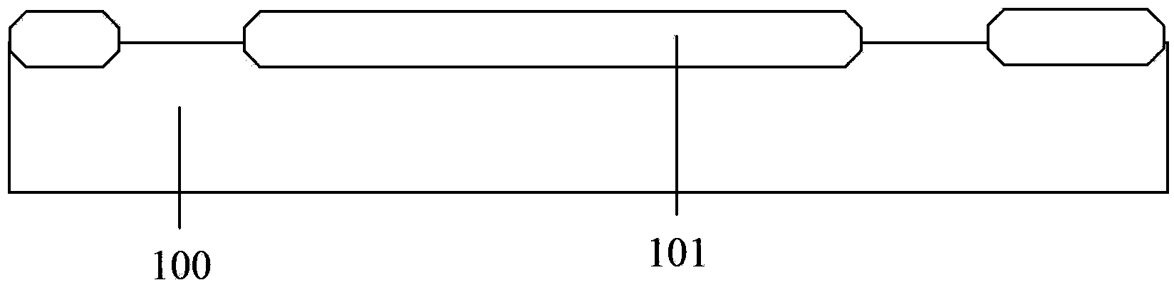
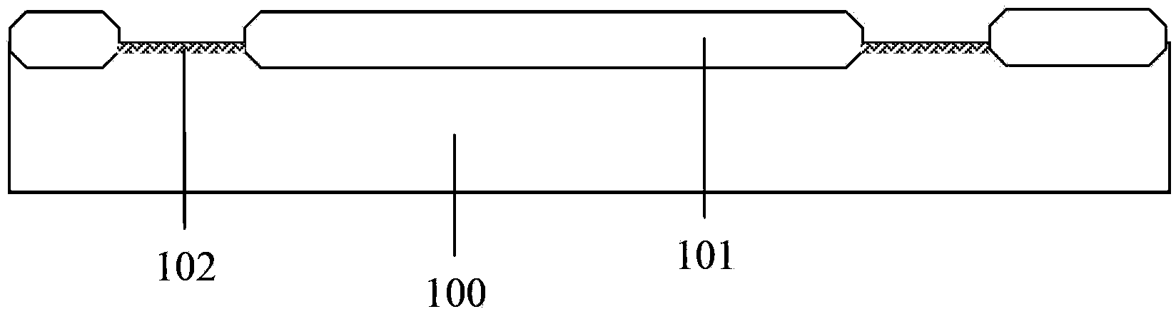
[0042] The preparation process of a Schottky diode of the present invention includes two parts of the process, as shown in Figures A1-A5: including a silicon substrate 100, a field silicon dioxide 101, a titanium silicide 102, a first dielectric 103, and a second dielectric 104 , Tungsten plug 105.

[0043] Figures A1 to A5 described in the present invention are the process of making the substrate by the existing standard submicron or deep submicron CMOS / BiCMOS process: the function of the substrate is to provide the negative pole and contact of the Schottky diode, the substrate 100 is the negative pole, and the negative pole contacts It is composed of titanium silicide 102 and tungsten plug 105 .

[0044] As shown in Figures B1 to B7: it includes a first photoresist 106, a metal titanium 107, a metal titanium nitride 108, a Schottky silicide 109, a metal cond...


PUM

PropertyMeasurementUnit
thicknessaaaaaaaaaa
thicknessaaaaaaaaaa
thicknessaaaaaaaaaa

Abstract

The invention relates to a process for producing a schottky diode which is compatible to a complementary metal oxide semiconductor (CMOS) / bipolar complementary metal oxide semiconductors (BiCMOS) process of a self alignment silicide technology. The method comprises the following steps of: a, providing a substrate technological wafer which has a formed contact hole tungsten plug; b, forming a schottky porose area on the substrate wafer through an etching technology; c, adopting a corrosion technology to remove the medium on the schottky porose area and silicon dioxide in the area, and enabling the substrate surface which corresponds to the schottky porose area to be exposed; d, removing a photoresist, cleaning, settling metallic titanium and titanium nitride, quickly thermal annealing, and forming a titanic schottky contact silicide; e, settling a metallic conducting layer; and f, metallic photoetching and corroding, and leading a schottky positive pole and a schottky negative pole out. The technology is simple to operate, and is used for solving the integration problem of the schottky diode for the CMOS / BiCMOS process of the self alignment silicide technology.

Description

technical field [0001] The invention relates to a process method for preparing Schottky diodes compatible with a submicron or deep submicron CMOS / BiCMOS process using self-aligned titanium silicide technology, and belongs to the technical field of semiconductor process manufacturing. Background technique [0002] Schottky diodes are generally formed by noble metals (such as aluminum, gold, platinum, tungsten, cobalt, nickel, titanium, etc.) Metals include aluminum, titanium, cobalt, nickel, etc. Among them, the junction formed by titanium is the most stable, and it is a metal commonly used in the Schottky process. For the Ti Schottky structure, whether it is a Schottky discrete device or a Schottky integrated circuit, the Schottky process is to deposit titanium and titanium nitride in the active region of the N-type semiconductor, and then pass appropriate rapid thermal Annealing process, forming Schottky contacts, followed by sputtering metal aluminum leads. However, for ...

Claims


Application Information

Patent Timeline
Patent Type & Authority Patents(China)
IPC IPC(8): H01L21/329
Inventor 郑若成
Owner 58TH RES INST OF CETC
Why Eureka
Try Eureka