Silicon on insulator (SOI) SiGe bipolar complementary metal oxide semiconductor (BiCMOS) integrated device and preparation method thereof

An integrated device and device technology, which is applied in the preparation of SOI SiGe BiCMOS integrated devices and the field of preparation, can solve problems such as affecting device performance, difficult to meet design, and inability to meet low power consumption and other problems

Inactive Publication Date: 2012-11-28
XIDIAN UNIV
View PDF3 Cites 3 Cited by
  • Summary
  • Abstract
  • Description
  • Claims
  • Application Information

AI Technical Summary

Problems solved by technology

For example, when the feature size is less than 100nm, due to problems such as tunneling leakage current and reliability, the traditional gate dielectric material SiO 2 It cannot meet the requirements of low power consumption; the short channel effect and narrow channel e...

Method used


Image

  • Silicon on insulator (SOI) SiGe bipolar complementary metal oxide semiconductor (BiCMOS) integrated device and preparation method thereof

Examples


Embodiment 1

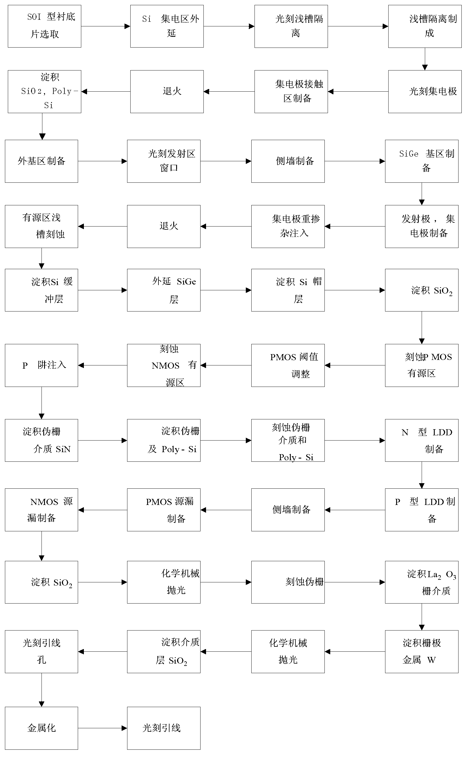
[0120] Embodiment 1: the preparation channel length is the SOI SiGe BiCMOS integrated device and the circuit of 22nm, concrete steps are as follows:

[0121] Step 1, epitaxial growth.

[0122] (1a) Select the SOI substrate, the support material of the lower layer of the substrate is Si, and the middle layer is SiO 2 , with a thickness of 150nm, and the upper material is doped with a concentration of 1×10 16 cm -3 N-type Si with a thickness of 100nm;

[0123] (1b) Using chemical vapor deposition (CVD), grow a layer of N-type epitaxial Si layer with a thickness of 50nm on the upper Si material at 600°C, as the collector region, and the doping concentration of this layer is 1× 10 16 cm -3 .

[0124] Step 2, shallow trench isolation preparation.

[0125] (2a) Using chemical vapor deposition (CVD), grow a layer of SiO with a thickness of 300 nm on the surface of the epitaxial Si layer at 600 °C. 2 Floor;

[0126] (2b) Photolithographic shallow trench isolation area;

[0...

Embodiment 2

[0183] Embodiment 2: the preparation channel length is the SOI SiGe BiCMOS integrated device and the circuit of 130nm, and concrete steps are as follows:

[0184] Step 1, epitaxial growth.

[0185] (1a) Select the SOI substrate, the support material of the lower layer of the substrate is Si, and the middle layer is SiO 2 , with a thickness of 300nm, and the upper material is doped with a concentration of 5×10 16 cm -3 N-type Si with a thickness of 120nm;

[0186](1b) Using chemical vapor deposition (CVD), grow an N-type epitaxial Si layer with a thickness of 80nm on the upper Si material at 700°C as the collector region, and the doping concentration of this layer is 5× 10 16 cm -3 .

[0187] Step 2, shallow trench isolation preparation.

[0188] (2a) Using chemical vapor deposition (CVD), grow a layer of SiO with a thickness of 400 nm on the surface of the epitaxial Si layer at 700 °C. 2 Floor;

[0189] (2b) Photolithographic shallow trench isolation area;

[0190] ...

Embodiment 3

[0246] Embodiment 3: the preparation channel length is the SOI SiGe BiCMOS integrated device and the circuit of 350nm, and concrete steps are as follows:

[0247] Step 1, epitaxial growth.

[0248] (1a) Select the SOI substrate, the support material of the lower layer of the substrate is Si, and the middle layer is SiO 2 , with a thickness of 400nm, and the upper material is doped with a concentration of 1×10 17 cm -3 N-type Si with a thickness of 150nm;

[0249] (1b) Using the method of chemical vapor deposition (CVD), grow a layer of N-type epitaxial Si layer with a thickness of 100nm on the upper layer of Si material at 750°C, as the collector region, and the doping concentration of this layer is 1× 10 17 cm -3 .

[0250] Step 2, shallow trench isolation preparation.

[0251] (2a) Using chemical vapor deposition (CVD), grow a layer of SiO with a thickness of 500 nm on the surface of the epitaxial Si layer at 800 °C. 2 Floor;

[0252] (2b) Photolithographic shallow...


PUM

PropertyMeasurementUnit
Thicknessaaaaaaaaaa
Thicknessaaaaaaaaaa
Thicknessaaaaaaaaaa

Abstract

The invention discloses a silicon on insulator (SOI) SiGe bipolar complementary metal oxide semiconductor (BiCMOS) integrated device and a preparation method of the SOI SiGe BiCMOS integrated device. The method comprises the following steps of: growing an N-type Si epitaxial layer on an SOI substrate, preparing shallow-trench isolation, forming a collector contact region, etching to form a side wall, performing wet etching to form a base region window, selectively growing a SiGe base region, photoetching a collector window, depositing an N-type Poly-Si, removing the Poly-Si, and forming a SiGe HBT device; growing a strain SiGe material on the substrate, isolating an active region of the device, photoetching an active region of an N-channel metal oxide semiconductor (NMOS) device, performing P-type ion implantation, preparing a pseudo grid, self-aligning to grow a source drain region of a metal oxide semiconductor (MOS) device, removing the pseudo grid, preparing a lanthanum oxide material to form gate dielectric and preparing metal tungsten to form a gate in a stamping groove at the pseudo grid, photoetching a lead, and preparing the integrated device and the circuit. According to the method, the characteristics of SiGe are fully utilized, and due to the prepared integrated circuit, the performance of the conventional analog and digital/analog mixed integrated circuit is greatly improved.

Description

technical field [0001] The invention belongs to the technical field of semiconductor integrated circuits, and in particular relates to a method for preparing an SOI SiGe BiCMOS integrated device and a preparation method. Background technique [0002] Semiconductor integrated circuit technology is the core technology of high-tech and information industries, and has become an important symbol to measure a country's scientific and technological level, comprehensive national strength and national defense strength, while microelectronic technology represented by integrated circuits is the key to semiconductor technology. The semiconductor industry is the basic industry of the country. The reason why it develops so fast is not only the huge contribution of technology itself to economic development, but also its wide applicability. [0003] Gordon Moore, one of the founders of Intel, proposed "Moore's Law" in 1965, which states that the number of transistors on an integrated circui...

Claims


Application Information

Patent Timeline
IPC IPC(8): H01L27/12H01L21/84
Inventor 张鹤鸣周春宇宋建军胡辉勇王海栋宣荣喜李妤晨郝跃
Owner XIDIAN UNIV
Why Eureka
Try Eureka