Method for manufacturing coaxial silicon carbide/silicon dioxide nanocable with chemical vapor deposition method
A technology of chemical vapor deposition and silicon dioxide, applied in gaseous chemical plating, cable/conductor manufacturing, circuit, etc., can solve problems such as difficult control, complex process, poor product purity and uniformity, and reduce production cost , simple synthesis process and low equipment requirements
- Summary
- Abstract
- Description
- Claims
- Application Information
AI Technical Summary
Problems solved by technology
Method used
Image
Examples
example 1
[0026] Make the density about 1.70g / cm 3 The carbon / carbon composite material is processed into 20×10×5mm 3 The sample was polished with No. 800 and No. 1000 sandpaper in turn, then ultrasonically cleaned with distilled water, dried in an oven at 120°C, and soaked in a 50% nickel nitrate aqueous solution until there were no air bubbles on the surface of the sample. The sample was then dried in an oven at 80°C as a deposition substrate.
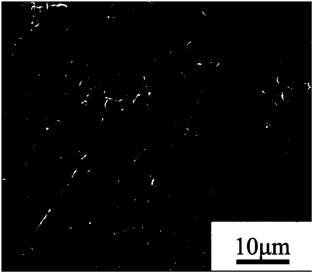
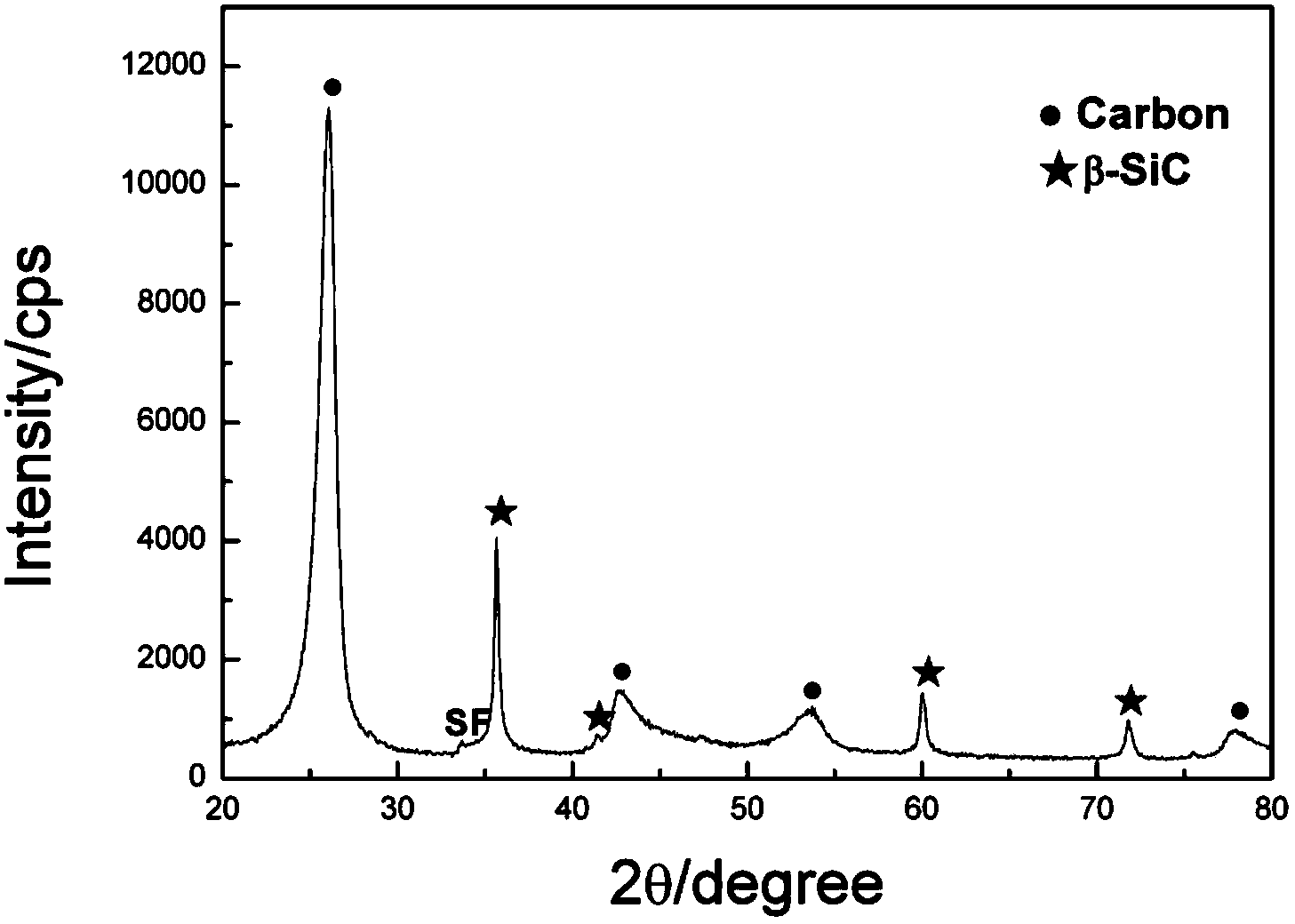
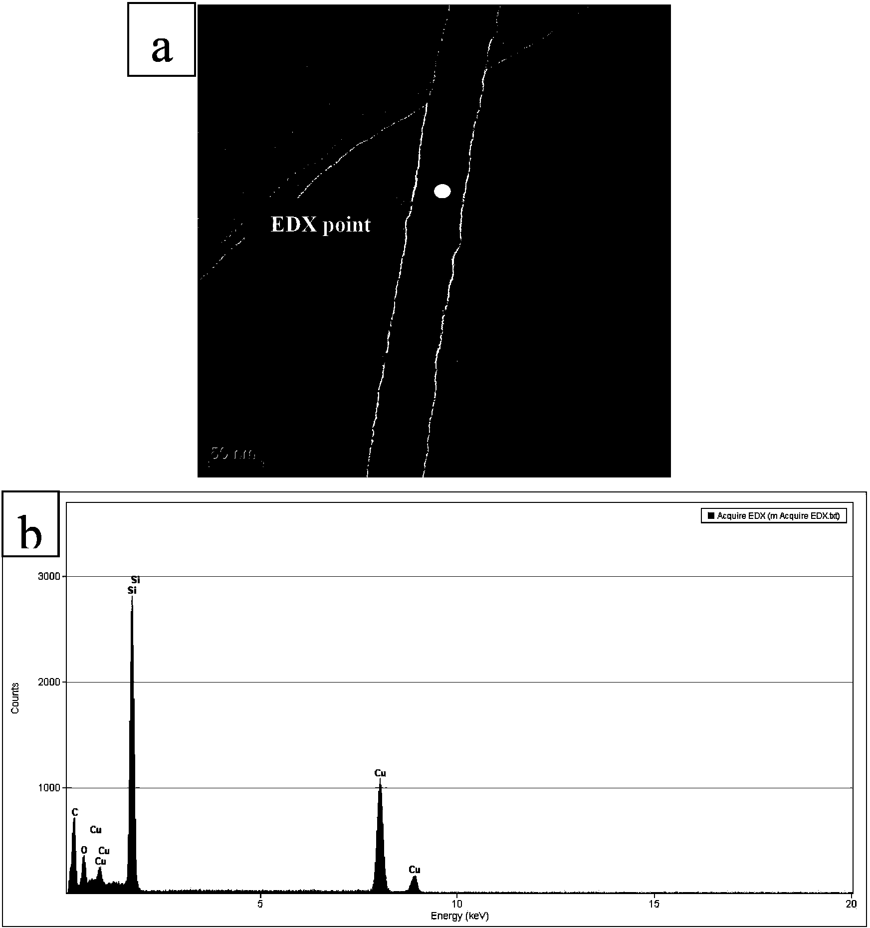
[0027] The soaked carbon / carbon composite material is bound with a bundle of carbon fibers and hung in the deposition area of a vertical chemical vapor deposition furnace. Vacuum the deposition furnace to 2000 Pa, keep the vacuum for 30 minutes to confirm that the sealing performance of the deposition furnace is intact, and then pass argon gas to normal pressure, and repeat this process three times. Then, the temperature of the deposition furnace was raised to 1100 °C at a rate of 10 °C / min. During the heating process, argon gas was flowed...
example 2
[0030] Make the density about 1.70g / cm 3 The carbon / carbon composite material is processed into 20×10×5mm 3 The sample was polished with No. 800 and No. 1000 sandpaper in turn, then ultrasonically cleaned with distilled water, dried in an oven at 120°C, and soaked in a 50% nickel nitrate aqueous solution until there were no air bubbles on the surface of the sample. The sample was then dried in an oven at 80°C as a deposition substrate.
[0031] The soaked carbon / carbon composite material is bound with a bundle of carbon fibers and hung in the deposition area of a vertical chemical vapor deposition furnace. Vacuum the deposition furnace to 2000 Pa, keep the vacuum for 30 minutes to confirm that the sealing performance of the deposition furnace is intact, and then pass argon gas to normal pressure, and repeat this process three times. Then the deposition furnace was heated up to 1300°C at a rate of 10°C / min. During the heating process, argon gas was flowed into the depositio...
example 3
[0034] Make the density about 1.70g / cm 3 The carbon / carbon composite material is processed into 20×10×5mm 3 The sample was polished with No. 800 and No. 1000 sandpaper in turn, and then ultrasonically washed with distilled water. After drying in an oven at 120°C, it was soaked in a nickel nitrate aqueous solution with a mass percentage of 15% until there were no air bubbles on the surface of the sample. The sample was then dried in an oven at 80°C as a deposition substrate.
[0035] The soaked carbon / carbon composite material is bound with a bundle of carbon fibers and hung in the deposition area of a vertical chemical vapor deposition furnace. Vacuum the deposition furnace to 2000 Pa, keep the vacuum for 30 minutes to confirm that the sealing performance of the deposition furnace is intact, and then pass argon gas to normal pressure, and repeat this process three times. Then, the temperature of the deposition furnace was raised to 1100 °C at a rate of 10 °C / min. During th...
PUM
| Property | Measurement | Unit |
|---|---|---|
| density | aaaaa | aaaaa |
| diameter | aaaaa | aaaaa |
Abstract
Description
Claims
Application Information
 - R&D
- Intellectual Property
- Life Sciences
- Materials
- Tech Scout
- Unparalleled Data Quality
- Higher Quality Content
- 60% Fewer Hallucinations
Browse by: Latest US Patents, China's latest patents, Technical Efficacy Thesaurus, Application Domain, Technology Topic, Popular Technical Reports.
© 2025 PatSnap. All rights reserved.Legal|Privacy policy|Modern Slavery Act Transparency Statement|Sitemap|About US| Contact US: help@patsnap.com


