

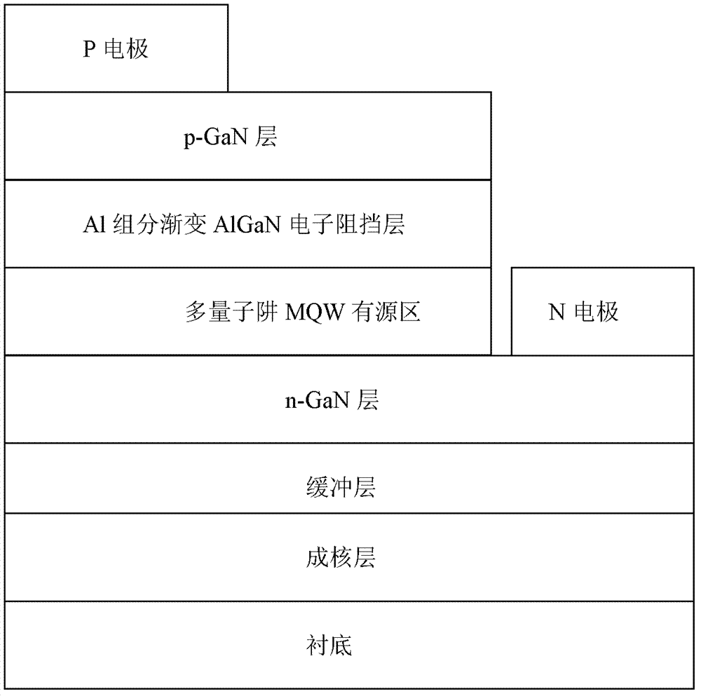
LED structure with aluminum-component-gradient electron blocking layer
A technology of electron blocking layer and aluminum component, which is applied in the field of optoelectronics, can solve the problems of reduced internal quantum efficiency and band bending, and achieve the effects of weakening energy band bending, weakening potential barriers, and improving carrier injection efficiency
- Summary
- Abstract
- Description
- Claims
- Application Information
AI Technical Summary
Problems solved by technology
Method used
Image

Examples
Embodiment 1
[0052] The invention utilizes the MOCVD growth technology to grow the LED epitaxial structure containing graded Al composition EBL on the sapphire substrate. Specifically include the following steps:
[0053] 1) Nucleation layer and buffer layer: In the MOCVD reaction chamber, the substrate was heated to 1100°C, treated in a hydrogen atmosphere for 5 minutes, and then the temperature was lowered to 530°C to grow a GaN nucleation layer with a thickness of 40nm; then the temperature was raised to At 1070°C, hydrogen is used as a carrier gas to grow a non-doped GaN buffer layer with a thickness of 3 μm;
[0054] 2) In the MOCVD reaction chamber, adjust the temperature to 1050°C and grow a Si-doped n-type GaN layer with a thickness of 3.5 μm. The doping concentration range of Si is: 5×10 18 cm -3 ;
[0055] 3) In the MOCVD reaction chamber, metal-organic sources TMGa and TMIn are introduced to grow multiple quantum well layers. The multiple quantum well layers are alternately g...
Embodiment 2
[0060] The invention utilizes the MOCVD growth technology to grow the LED epitaxial structure containing graded Al composition EBL on the sapphire substrate. Specifically include the following steps:
[0061] 1) Nucleation layer and buffer layer: In the MOCVD reaction chamber, the substrate was heated to 1100°C, treated in a hydrogen atmosphere for 5 minutes, and then the temperature was lowered to 530°C to grow a GaN nucleation layer with a thickness of 40nm; then the temperature was raised to At 1070°C, hydrogen is used as a carrier gas to grow a non-doped GaN buffer layer with a thickness of 3 μm;
[0062] 2) In the MOCVD reaction chamber, adjust the temperature to 1050°C and grow a Si-doped n-type GaN layer with a thickness of 3.5 μm. The doping concentration range of Si is: 5×10 18 cm -3 ;
[0063] 3) In the MOCVD reaction chamber, metal-organic sources TMGa and TMIn are introduced to grow multiple quantum well layers. The multiple quantum well layers are alternately g...
PUM
 Abstract
Description
Claims
Application Information