Method for preparing FinFET on germanium and III-V semiconductor material substrate

A technology of the third and fifth groups and semiconductors, which is applied in the manufacture of semiconductor/solid-state devices, semiconductor devices, electrical components, etc., and can solve the problems of adjusting threshold voltage, small on-state current, and high process cost

Inactive Publication Date: 2012-12-19
PEKING UNIV
View PDF8 Cites 4 Cited by
  • Summary
  • Abstract
  • Description
  • Claims
  • Application Information

AI Technical Summary

Problems solved by technology

But its disadvantages are: (1) The process cost is too high, and the SOI substrate is quite expensive; (2) The source-drain lifting technology is required, otherwise the extended resistance of the source and drain is too large, resulting in too small on-state current and poor device performance; (3) There is no body extraction, so the threshold voltage cannot be adjusted through the substrate bias effect

Method used


Image

  • Method for preparing FinFET on germanium and III-V semiconductor material substrate
  • Method for preparing FinFET on germanium and III-V semiconductor material substrate
  • Method for preparing FinFET on germanium and III-V semiconductor material substrate

Examples


Embodiment Construction

[0041]The present invention will be described in detail below in conjunction with the accompanying drawings and specific embodiments, and a process scheme for manufacturing FinFETs on germanium and III-V semiconductor material substrates proposed in the present invention will be specifically given, but the scope of the present invention is not limited in any way.

[0042] According to the following steps, plan 1 for n-type germanium and Group III and V FinFETs with a Fin strip thickness of about 20 nanometers and a channel length of about 32 nanometers:

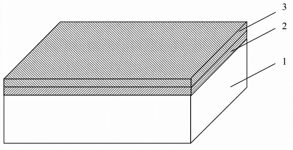
[0043] 1. Ion-enhanced chemical vapor deposition of silicon oxide 300 on a silicon substrate

[0044] 2. Ion-enhanced chemical vapor deposition of silicon nitride 1000 on silicon oxide Such as figure 1 shown;

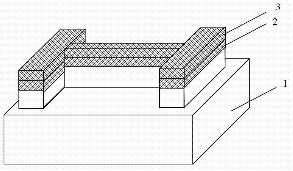
[0045] 3. Electron beam lithography defines the source and drain and the thin strip pattern structure connecting the source and drain, wherein the width of the thin strip pattern structure is 20 nanometers;

[0...


PUM

PropertyMeasurementUnit
widthaaaaaaaaaa

Abstract

The invention discloses a method for preparing FinFET on a germanium and III-V semiconductor material substrate, and the method mainly comprises following steps of forming a source drain and a slender graphic structure which is connected to the source drain; forming an oxidization isolation layer; forming a grid structure and a source drain structure; and forming metal contact and metal interconnection. Due to the adoption of the method, the FinFET is easily formed on the germanium and III-V semiconductor material substrate, the entire process flow is completed on the germanium and III-V semiconductor material substrate and is completely similar to the manufacturing technology of a conventional ultra-large-sized integrated structure, and the preparation process has characteristics of simpleness, convenience and short period. In addition, the minimal width of the FinFET prepared by the method can be controlled within 20 nanometers, and a multi-grid structure can provide good grid control capacity and is very suitable for preparing ultra-short-channel devices to further reduce the size of the devices. The FinFET prepared by the method has low power consumption.

Description

technical field [0001] The invention provides a method for preparing a FinFET on a germanium and III-V semiconductor material substrate, and belongs to the technical field of VLSI manufacturing. Background technique [0002] Today's semiconductor manufacturing industry is developing rapidly under the guidance of Moore's Law, continuously improving the performance and integration density of integrated circuits, while reducing the power consumption of integrated circuits as much as possible. Therefore, the preparation of ultra-short trench devices with high performance and low power consumption will become the focus of the future semiconductor manufacturing industry. After entering the 22nm technology node, the leakage current of traditional planar field effect transistors continues to increase, as well as the increasingly serious short channel effect and leakage-induced barrier lowering (DIBL) effect, which cannot be well adapted to the development of semiconductor manufactur...

Claims


Application Information

Patent Timeline
Patent Type & Authority Applications(China)
IPC IPC(8): H01L21/336
CPCH01L29/66795H01L21/02164H01L21/0217H01L21/0228H01L21/0277H01L21/0332H01L21/28194H01L21/2855H01L21/28556H01L21/31055H01L21/31111H01L21/31116H01L21/3212H01L21/324
Inventor 黄如樊捷闻许晓燕李佳王润声
Owner PEKING UNIV
Why Eureka
Try Eureka