

Electrochromism device and preparation method thereof
An electrochromic and electrochromic layer technology, applied in the direction of instruments, nonlinear optics, optics, etc., can solve the problems such as hindering the application of electrochromic devices, long time spent in coloring or fading, etc., and shortening the time of discoloration , good stability, the effect of increasing the conduction velocity
- Summary
- Abstract
- Description
- Claims
- Application Information
AI Technical Summary
Problems solved by technology
Method used
Image

Examples
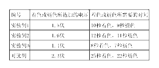
Embodiment 1
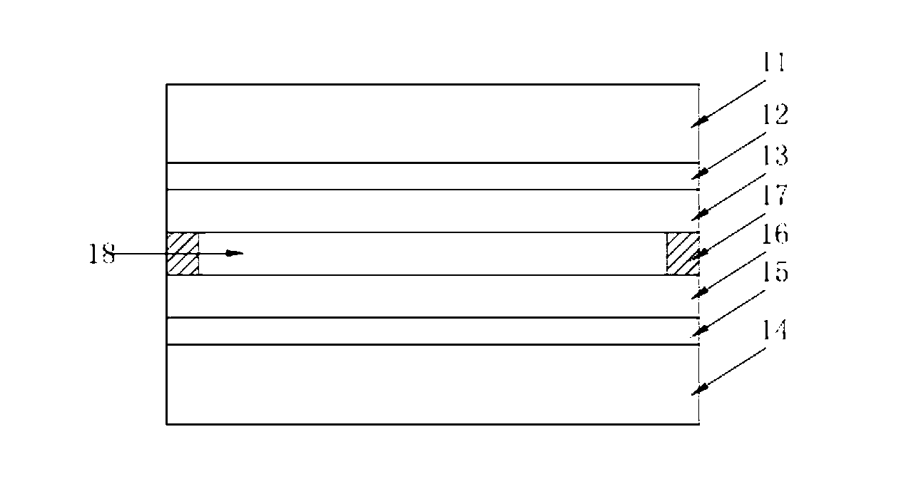
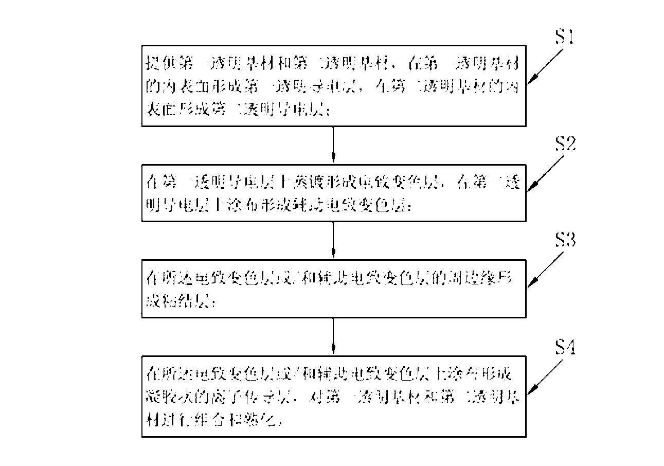
[0054] S1. Coating a layer of indium tin oxide (ITO) on the first transparent substrate glass with a thickness of 1.1 mm to form a first transparent conductive layer with a resistance value of 15 ohms / □; on the second transparent substrate with a thickness of 0.175 mm A layer of indium tin oxide (ITO) was plated on the material polyethylene terephthalate to form a second transparent conductive layer with a resistance value of 80 ohms / □.
[0055] S2. Vacuum-deposit a layer of tungsten oxide (WO3) on the first transparent conductive layer to form an electrochromic layer, thereby forming the first unit of the electrochromic device, which is expressed as [Glass / ITO / WO3]; A thin film of titanium oxide-cerium oxide (TiO2-CeO2) is coated on the second transparent conductive layer to form an auxiliary electrochromic layer, thereby forming the second unit of the electrochromic device, and expressed as [PET / ITO / TiO2—CeO2].
[0056] S3. Coating an epoxy resin on the periphery of the el...
Embodiment 2
[0063] S1. Coating a layer of indium tin oxide (ITO) on the first transparent substrate glass with a thickness of 1.1 mm to form a first transparent conductive layer with a resistance value of 15 ohms / □; on the second transparent substrate with a thickness of 0.188 mm A layer of tin oxide was plated on polymethyl methacrylate to form a second transparent conductive layer with a resistance value of 30 ohms / □.
[0064]S2. Vacuum-deposit a layer of molybdenum oxide on the first transparent conductive layer to form an electrochromic layer, thus forming the first unit of the electrochromic device; coating a layer of vanadium oxide thin film on the second transparent conductive layer , to form an auxiliary electrochromic layer, thereby forming the second unit of the electrochromic device.
[0065] S3. Using a dispenser to coat an epoxy resin on the periphery of the electrochromic layer to form a bonding layer.
[0066] S4. Coating and forming a gel-like ion-conducting layer on the ...
Embodiment 3
[0072] S1. Coating a layer of indium tin oxide (ITO) on the first transparent substrate glass with a thickness of 1.1 mm to form a first transparent conductive layer with a resistance value of 15 ohms / □; on the second transparent substrate with a thickness of 0.18 mm A layer of zinc oxide is plated on the material polycarbonate to form a second transparent conductive layer with a resistance value of 80 ohm / □.
[0073] S2. Vacuum-deposit a layer of iridium oxide on the first transparent conductive layer to form an electrochromic layer, thus forming the first unit of the electrochromic device; coating a layer of nickel oxide film on the second transparent conductive layer , to form an auxiliary electrochromic layer, thereby forming the second unit of the electrochromic device.
[0074] S3. Apply an epoxy resin on the peripheral edge of the auxiliary electrochromic layer by using a dispenser to form a bonding layer.
[0075] S4. Coating and forming a gel-like ion-conducting laye...
PUM
 Abstract
Description
Claims
Application Information