epitaxial wafer structure of gallium nitride-based LED (Light-Emitting Diode) and preparation method thereof

A light-emitting diode, gallium nitride-based technology, applied in electrical components, circuits, semiconductor devices, etc., can solve the problems of decreasing radiation recombination efficiency, reducing the internal quantum efficiency of LEDs, etc., to achieve the effect of increasing the light-emitting area

Active Publication Date: 2012-12-26
EPITOP PHOTOELECTRIC TECH
View PDF4 Cites 21 Cited by
  • Summary
  • Abstract
  • Description
  • Claims
  • Application Information

AI Technical Summary

Problems solved by technology

[0009] The purpose of the present invention is to overcome the extremely strong polarization field in the active layer in the traditional LED device structure, which makes the energy band of the quantum well tilt, and the electron-hole wave function is separated in space, so that the radiation recombination efficiency is reduced. Thereby reducing the problem of LED internal quantum efficiency, providing a gallium nitride-based light-emitting diode epitaxial wafer structure with better crystal quality and non-planar active layer structure on the weak polar surface and its preparation method

Method used


Image

  • epitaxial wafer structure of gallium nitride-based LED (Light-Emitting Diode) and preparation method thereof
  • epitaxial wafer structure of gallium nitride-based LED (Light-Emitting Diode) and preparation method thereof
  • epitaxial wafer structure of gallium nitride-based LED (Light-Emitting Diode) and preparation method thereof

Examples


Embodiment Construction

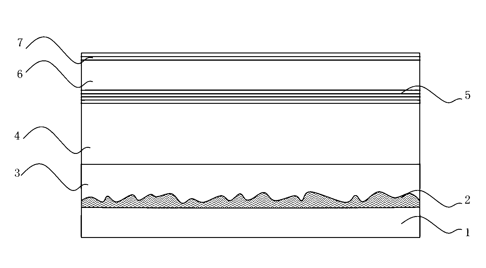
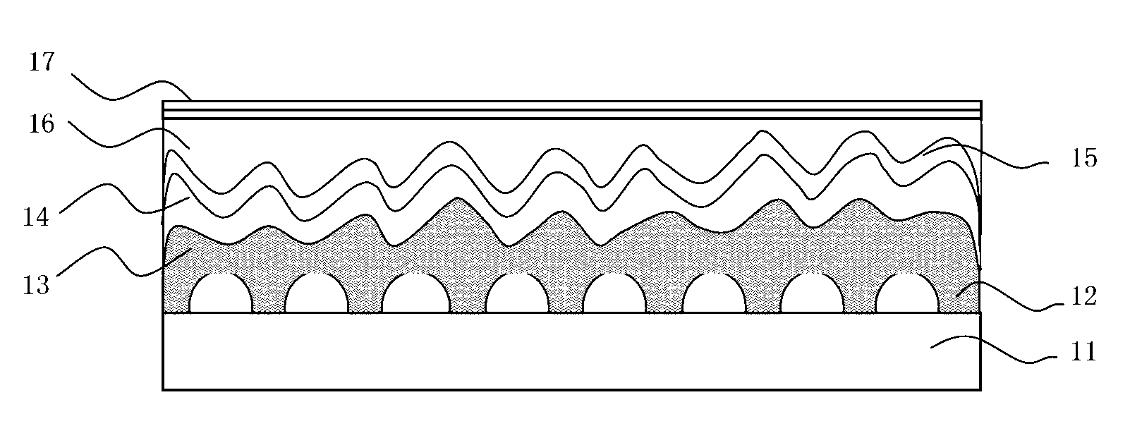
[0026] The specific implementation of the structure of a GaN-based light-emitting diode epitaxial wafer on a weakly polar surface and its preparation method provided by the present invention will be described in detail below with reference to the accompanying drawings.

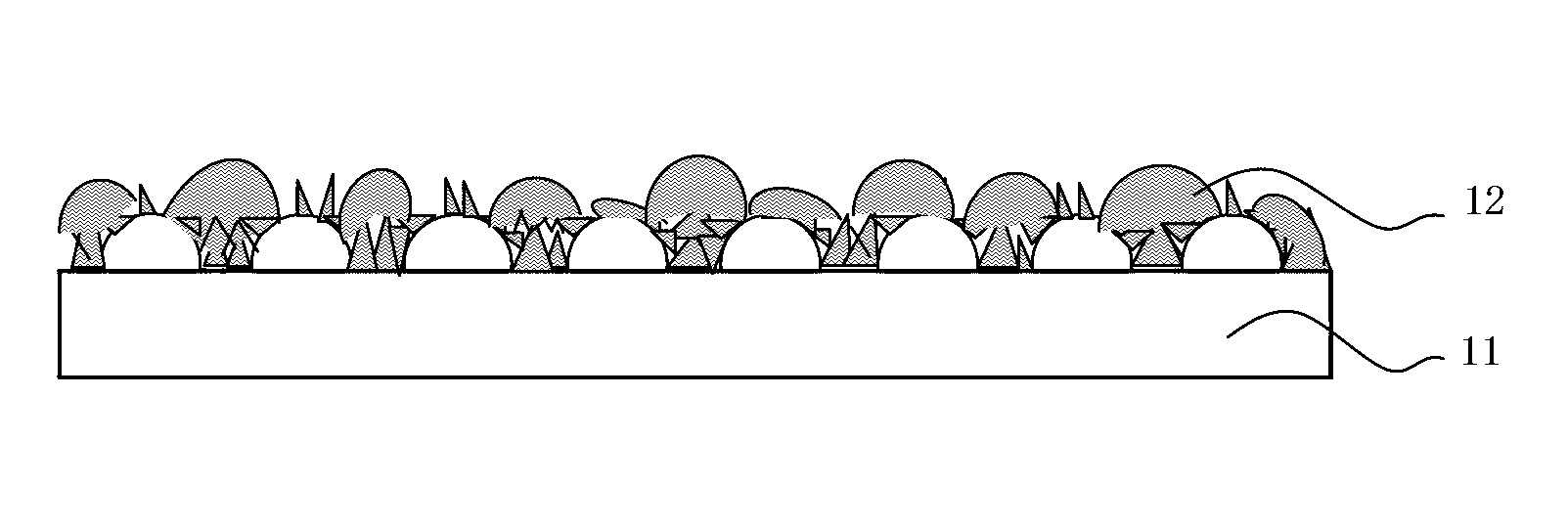
[0027] attached figure 2 And attached image 3 Shown is a schematic diagram of the process of the method of the present invention. The specific steps of the method for preparing the epitaxial wafer structure of a gallium nitride-based light-emitting diode on a weakly polar surface according to the present invention are as follows:

[0028] 1) Load the graphic substrate 11 into the reaction chamber, and 2 Heating to above 1050°C in the atmosphere for heat treatment of the substrate for 10-20 minutes; then cooling down at 500-650°C to grow a nucleation layer with a thickness of 15-100nm, the material is Al x In y Ga 1-x-y N, where 0≤X≤1, 0≤Y≤1.

[0029] 2) High-temperature annealing at 900-1100°C to obtain...


PUM


Abstract

The invention relates to a process of growing a nucleating layer on the surface of a patterned substrate at a low temperature to form an uneven surface. The invention overcomes the problem that in a conventional LED (Light-Emitting Diode) device structure, an active layer has a superstrong depolarization field, and thus, an energy band of a quantum well is inclined, an electron hole wave function is separated in space and the radiative recombination efficiency is reduced, so that the internal quantum efficiency of a LED is reduced. The invention also provides an epitaxial wafer structure of a gallium nitride-based LED and a preparation method of the epitaxial wafer structure, wherein the epitaxial wafer structure has high crystalline quality and a nonplanar active layer structure is implemented on a weak polarity surface of the epitaxial wafer structure. Therefore, the internal quantum efficiency of the LED is improved.

Description

technical field [0001] The present invention relates to the field of semiconductor optoelectronic devices, in particular to a method for obtaining a gallium nitride-based light-emitting diode epitaxial wafer with a non-planar and weakly polar surface active layer on a weakly polar surface using the epitaxial growth technology of compound semiconductor thin films . Background technique [0002] Semiconductor LED will become the next generation of daily lighting source, which has become the consensus of governments, scientific and technological circles and industry circles all over the world. It is a new generation of "green lighting" light source in the 21st century after incandescent lamps and fluorescent lamps. It has many advantages such as energy saving and environmental protection, long life, small size and rich colors, and its realization as a daily lighting source will generate great social and economic benefits. [0003] At present, the luminous efficiency of white L...

Claims


Application Information

Patent Timeline
Patent Type & Authority Applications(China)
IPC IPC(8): H01L33/00H01L33/22H01L33/04
Inventor 陈静
Owner EPITOP PHOTOELECTRIC TECH
Why Eureka
Try Eureka