Split-grid type metal-oxide-semiconductor field effect transistor (MOSFET) imaging detector and operating method thereof

An imaging detector and split gate technology, applied in image communication, TV, color TV components, etc., can solve the problems of difficult to continue to improve resolution, pixel size limitation, and extremely small pixel size

Active Publication Date: 2013-01-02
NANJING UNIV
View PDF6 Cites 15 Cited by
  • Summary
  • Abstract
  • Description
  • Claims
  • Application Information

AI Technical Summary

Problems solved by technology

However, from a structural point of view, this imaging device actually uses three transistors (two MOS transistors and a floating gate MOS transistor) as a pixel unit, and the pixel size is limited, so it is difficult to achieve extreme With small pixels, it is difficult to continue to improve the resolution

Method used


Image

  • Split-grid type metal-oxide-semiconductor field effect transistor (MOSFET) imaging detector and operating method thereof
  • Split-grid type metal-oxide-semiconductor field effect transistor (MOSFET) imaging detector and operating method thereof
  • Split-grid type metal-oxide-semiconductor field effect transistor (MOSFET) imaging detector and operating method thereof

Examples


Embodiment Construction

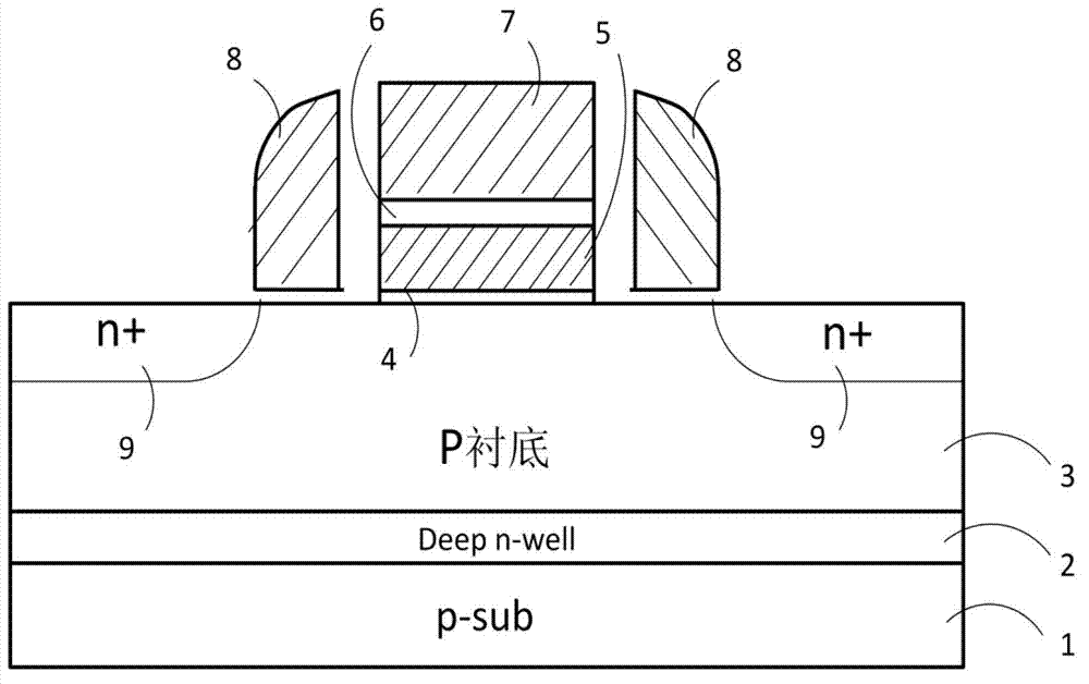
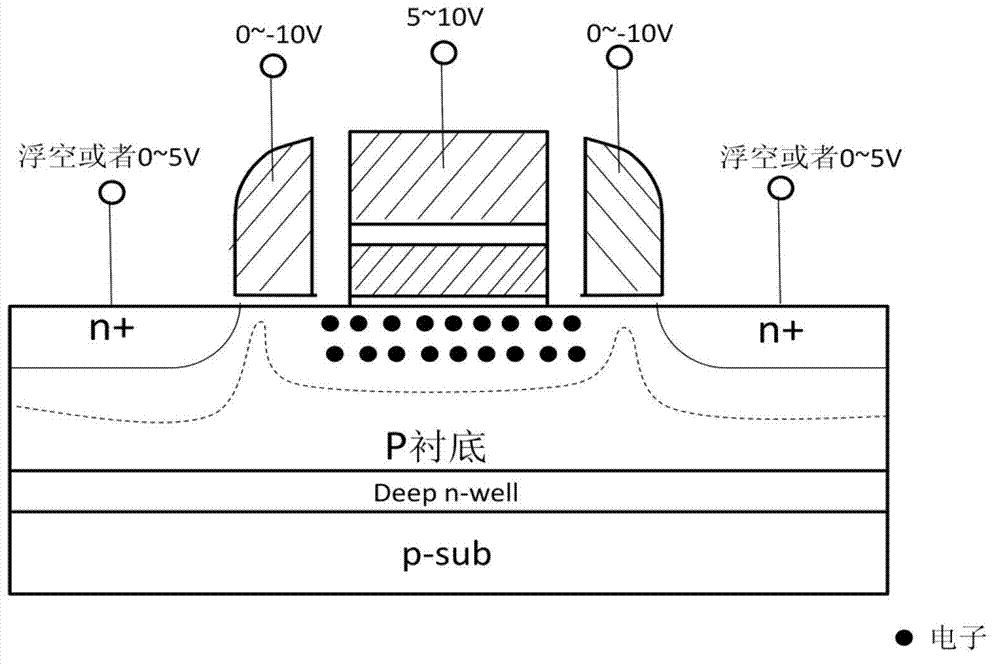
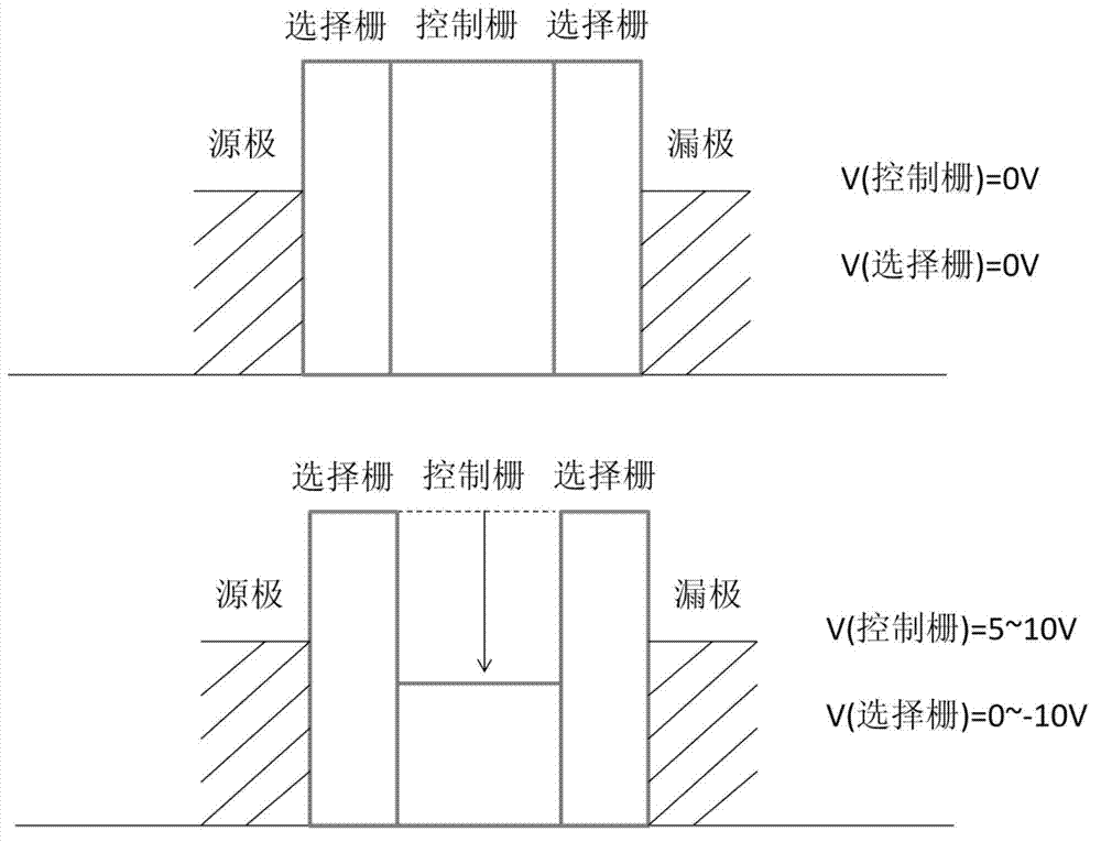
[0043] The split gate type MOSFET imaging detector of the present invention, the composition of its unit device figure 1 As shown, the details are as follows: a deep N-type well (2) is implanted on a P-type semiconductor silicon wafer (1), and a P-type well (3) is implanted on the deep N-type well to form a split-gate MOSFET imaging detection device substrate. The split-gate MOSFET includes a floating gate MOSFET and two selection gates, and the two selection gates (8) are arranged on both sides of the floating gate MOSFET, connecting the substrate controlled by the control gate (7) and the imaging detector The source and drain (9) are separated.

[0044] The structure of the floating gate MOSFET is that two layers of insulating dielectric layers (4) and (6) are respectively arranged on the P-type substrate (3), and an optoelectronic storage layer (5) is arranged between the two layers of insulating dielectric layers. A control grid (7) is arranged directly above the dielect...


PUM


Abstract

The invention provides a split-grid type metal-oxide-semiconductor field effect transistor (MOSFET) imaging detector and an operating method thereof. The split-grid type MOSFET is structurally characterized in that two insulating medium layers and a control grid are arranged above a P-type substrate; a photoelectron storage layer is arranged between the two insulating medium layers; selection grids are arranged on two sides of the control grid; a substrate controlled by the control grid is separated from the source and drain of a probe; the insulating medium layer on the top of the substrate contacted with the control grid is a material for preventing the loss of electric charge stored in the photoelectron storage layer to the control grid; and a transparent or semitransparent window of the probe length of the probe is arranged at one of the surfaces of the substrate layer or the control grid. By utilizing the split-grid type MOSFET imaging detector, the collection efficiency of the photoelectron is effectively improved; the dark current of the probe is inhibited; and the detector is not sensitive to process defects, wide in dynamic range and high accuracy in signal reading.

Description

1. Technical field [0001] The present invention relates to a solid-state imaging detector device, in particular to the device structure and working mechanism of a solid-state imaging detector in the infrared, visible light band to ultraviolet band, and is a non-volatile imaging device with storage function based on a split gate structure MOSFET and its Operation method. 2. Background technology [0002] Image sensors are widely used in various fields such as military, civilian and national defense, such as digital cameras, mobile phones, and video cameras. The main solid-state imaging detectors currently developed are CCD imaging detectors and CMOS-APS. CCD appeared earlier, and now its production technology is relatively mature. Its basic structure is a series of MOS capacitors connected in series, and the generation and change of the semiconductor surface potential well are controlled by the voltage pulse sequence on the capacitor, thereby realizing the storage of photoge...

Claims


Application Information

Patent Timeline
Patent Type & Authority Applications(China)
IPC IPC(8): H01L27/146H04N5/335
Inventor 卜晓峰闫锋夏好广吴福伟马浩文司向东张佳辰
Owner NANJING UNIV
Why Eureka
Try Eureka