
Integrated waveguide filter of medium loaded foldable substrate

A substrate-integrated waveguide and dielectric loading technology, which is applied in the field of radio frequency and microwave, can solve the problems of increasing the resonator conductor and radiation loss, the difficulty of realizing the transmission zero point of the filter, reducing the size of the resonator cavity and the filter, etc., and achieving low insertion loss. , Improve parasitic suppression characteristics, small size effect

Inactive Publication Date: 2013-01-09
SHANGHAI JIAO TONG UNIV
View PDF4 Cites 19 Cited by
  • Summary
  • Abstract
  • Description
  • Claims
  • Application Information

AI Technical Summary

Problems solved by technology

Patent document number CN201120042595.9 "Substrate-integrated waveguide filter with steep sideband characteristics" proposes a filter with defective ground structure (DGS) resonators carved on the surface of the substrate-integrated waveguide, which has a small area and is There are transmission zeros on the left and right of the strip; however, slots on the metal plane will increase the conductor and radiation losses of the resonator, thereby increasing the filter insertion loss
[0004] In addition, Wu, L.-S. et al published the article "Bandpass Filter Using Substrate Integrated Waveguide Cavity Loaded With Dielectric Rod" in IEEE Microw.Wireless Compon.Lett. By loading a dielectric rod short-circuited at both ends in the middle of the traditional substrate-integrated rectangular resonator, the size of the resonator and filter is greatly reduced, the unloaded Q value and insertion loss performance are improved, and the parasitic suppression characteristics of the component are improved; but The filter is difficult to achieve the transmission zero, the area is still larger than the microstrip circuit

Method used


Image

  • Integrated waveguide filter of medium loaded foldable substrate
  • Integrated waveguide filter of medium loaded foldable substrate
  • Integrated waveguide filter of medium loaded foldable substrate

Examples


Embodiment Construction

[0028] The embodiments of the present invention are described in detail below. This embodiment is implemented on the premise of the technical solution of the present invention, and detailed implementation methods and specific operating procedures are provided, but the protection scope of the present invention is not limited to the following implementation example.

[0029] This embodiment is a fourth-order quasi-elliptic dielectric-loaded folded substrate integrated waveguide bandpass filter with a center frequency of 3.45 GHz, an equiripple bandwidth of 140 MHz, and an in-band reflection loss of 20 dB.

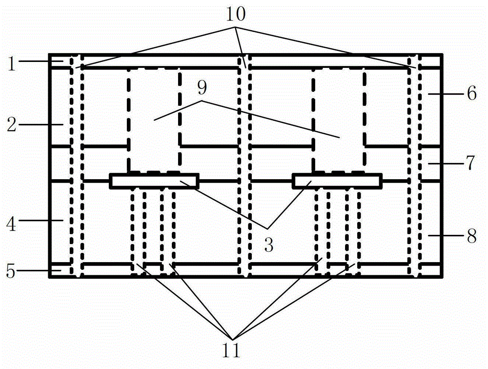
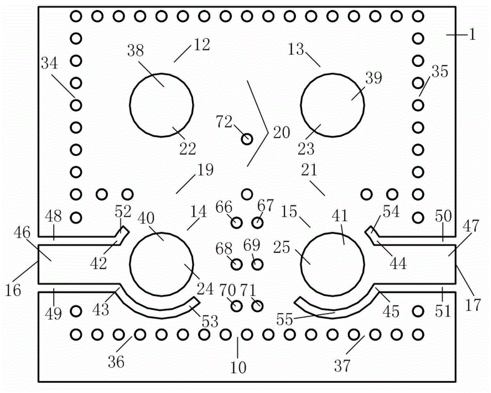
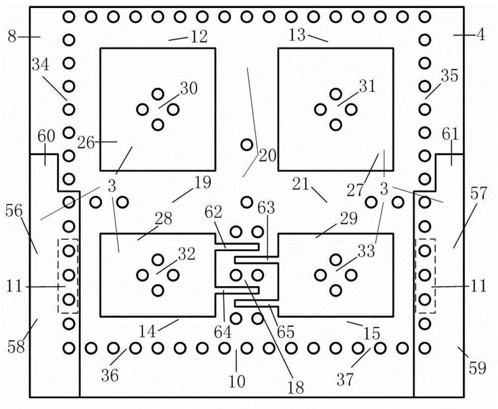
[0030] Such as figure 1As shown, the overall structure is composed of the first metal layer 1, the first dielectric layer 2, the second metal layer 3, the second dielectric layer 4 and the third metal layer 5 from top to bottom; the first dielectric layer 2 is composed of the second A dielectric substrate 6 and an adhesive 7 are stacked up and down; the second dielectric lay...


PUM


Abstract

The invention provides an integrated waveguide filter of a medium loaded foldable substrate. The integrated waveguide filter comprises a first metal layer, a first medium layer, a second metal layer, a second medium layer and a third metal layer from top to bottom, wherein a high-dielectric-constant and high-Q-value medium block is embedded into the first medium layer; and a metalized through hole and a blind hole array, which respectively penetrate through the whole structure and the second medium layer, are additionally arranged. The whole body is formed by three main parts including resonant cavity structures, a feeder line structure and a coupling structure. The quantity of the resonant cavity structures is the same as that of the step quantity of the filter; and each resonant cavity structure is formed by a metalized through hole group embedded into the periphery of a medium block and covering parts of the first metal layer and the second metal layer. The feeder line structure can be used for realizing loading land coplanar waveguide on a groove at the edge of the first metal layer. The coupling structure is divided into an inter-digital electric coupling structure for realizing electric coupling and an induction window magnetic coupling structure for realizing magnetic coupling, and is specifically adopted between adjacent resonant cavities according to the design requirements of the filter. The integrated waveguide filter has the characteristics of miniaturization, low inserting loss, high-frequency selectivity, easiness for machining and the like.

Description

technical field [0001] The invention relates to a device in the field of radio frequency microwave technology, in particular to a dielectric-loaded folded substrate integrated waveguide filter. Background technique [0002] A microwave filter is one of the most basic components in a radio frequency system for gating or blocking signals or power in a specific frequency band, and its performance directly affects the performance of the entire system. The high performance and miniaturization of microwave filters have always been the main trend of its technical development. Substrate-integrated waveguide (SIW) is a microwave and millimeter-wave structure that simulates metal waveguides on a substrate by using printed circuit board (PCB) or low-temperature co-fired ceramics (LTCC). Its size and performance are between metal waveguides and planar circuits. Among them, it has the advantages of small planarization, high unloaded quality factor (Q value), large power capacity, and ea...

Claims


Application Information

Patent Timeline
Patent Type & Authority Applications(China)
IPC IPC(8): H01P1/20H01P1/208
Inventor 吴林晟高铭见毛军发尹文言
Owner SHANGHAI JIAO TONG UNIV
Learn More