Multi-grid transistor and manufacturing method thereof

A technology of transistors and gates, applied in the field of multi-gate transistors and its manufacturing, can solve problems such as excessive fluctuation of threshold voltage, limited cost, and reduced response speed of devices, so as to reduce the series resistance of source and drain and avoid amorphization problem, the effect of reducing the barrier height

Active Publication Date: 2013-01-16
INST OF MICROELECTRONICS CHINESE ACAD OF SCI
View PDF12 Cites 16 Cited by
  • Summary
  • Abstract
  • Description
  • Claims
  • Application Information

AI Technical Summary

Problems solved by technology

[0002] As the semiconductor feature size continues to shrink toward the 22 / 15nm level, the negative effects brought about by the reduction of the gate width become more and more obvious, and the traditional planar transistor can no longer meet the requirements
First of all, in order to eliminate the short channel effect, P and B need to be heavily doped into the channel, which increases the threshold voltage of the device and reduces the carrier mobility in the channel, resulting in a decrease in the response speed of the device, and the ion implantation process is difficult to control , it is easy to cause adverse results such as excessive fluctuation of threshold voltage
Secondly, the traditional SiGe PMOS silicon strain technology is also facing a bottleneck. In the 32nm process node, the content of Ge element doped at the source and drain electrodes has already accounted for about 40%, and it is difficult to provide a higher degree of strain for the channel.
Third, the development of gate oxide thickness also highlights the bottleneck, and the speed of thickness reduction has been difficult to keep up with the pace of gate width reduction
Therefore, the damage caused by ion implantation is difficult to be repaired in the impurity-activated annealing process step
[0005] In addition, another method to reduce the source-drain parasitic series resistance is to thicken the fin-shaped source-drain region 3A / 3B by epitaxial growth to form a raised source-drain region or a thickened source-drain region. However, this selective epitaxial growth process Due to the complicated steps and limited manufacturing costs, it is difficult to manufacture mass products on a large scale
[0006] All in all, the current multi-gate transistors are difficult to effectively reduce the source-drain parasitic resistance, and the device performance cannot be further improved

Method used


Image

  • Multi-grid transistor and manufacturing method thereof
  • Multi-grid transistor and manufacturing method thereof
  • Multi-grid transistor and manufacturing method thereof

Examples


Embodiment Construction

[0034] The features and technical effects of the technical solution of the present invention will be described in detail below with reference to the accompanying drawings and in combination with schematic embodiments, and a multi-gate transistor capable of effectively reducing source-drain parasitic resistance and a manufacturing method thereof are disclosed. It should be pointed out that similar reference numerals represent similar structures, and the terms "first", "second", "upper", "lower" and the like used in this application can be used to modify various device structures or process steps . These modifications do not imply spatial, sequential or hierarchical relationships of the modified device structures or process steps unless otherwise specified.

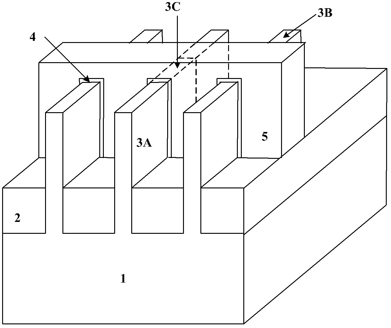
[0035] First, if image 3 As shown, a fin-shaped structure is formed. A semiconductor substrate 10 is provided, and its material may be bulk silicon or silicon-on-insulator (SOI), or bulk germanium or germanium-on-insulat...


PUM


Abstract

The invention discloses a multi-grid transistor, which comprises a substrate, an oxide layer positioned on the substrate, a fin-shaped structure which is positioned on the oxide layer, is connected with the substrate and comprises a trench region and a source region and a drain region which are positioned at two ends of the trench region, a grid dielectric layer which is positioned on the fin-shaped structure and wraps the trench region, and a grid which is positioned on the oxide layer and the grid dielectric layer and is perpendicular to the fin-shaped structure. The multi-grid transistor is characterized in that the source region and the drain region consist of metal silicate. According to a semiconductor device and a manufacturing method thereof, the metal silicate is completely used as the source region and the drain region of the fin-shaped structure of the multi-grid transistor, so that source and drain serially connected resistance is effectively reduced, and the problem that a non-crystallized region cannot be crystallized after being quenched because of doping of a source and a drain is solved; and furthermore, doped ion gathering regions are arranged at interfaces between the trench region and the metal silicate, so that the Schottky barrier height is effectively reduced, and the device performance is improved.

Description

technical field [0001] The invention relates to a semiconductor device and its manufacturing method, in particular to a multi-gate transistor and its manufacturing method. Background technique [0002] As the semiconductor feature size continues to shrink toward the level of 22 / 15nm, the negative effects brought about by the reduction of the gate width become more and more obvious, and the traditional planar transistor can no longer meet the requirements. First of all, in order to eliminate the short channel effect, P and B need to be heavily doped into the channel, which increases the threshold voltage of the device and reduces the carrier mobility in the channel, resulting in a decrease in the response speed of the device, and the ion implantation process is difficult to control , It is easy to cause adverse results such as excessive fluctuation of the threshold voltage. Secondly, the traditional SiGe PMOS silicon strain technology also faces a bottleneck. In the 32nm pro...

Claims


Application Information

Patent Timeline
Patent Type & Authority Applications(China)
IPC IPC(8): H01L29/78H01L29/08H01L21/336
Inventor 罗军赵超李俊峰
Owner INST OF MICROELECTRONICS CHINESE ACAD OF SCI
Why Eureka
Try Eureka