All-single-walled carbon nanotube field effect transistor and preparation method thereof

A single-walled carbon nanotube and field-effect transistor technology, which is applied in the field of all-single-walled carbon nanotube field-effect transistors and their preparation, can solve the problem that the performance stability of the device needs to be improved, the processing process is time-consuming and inefficient, and it is unfavorable for the direct preparation of the device. And other issues

Active Publication Date: 2013-01-30
INST OF METAL RESEARCH - CHINESE ACAD OF SCI
View PDF4 Cites 3 Cited by
  • Summary
  • Abstract
  • Description
  • Claims
  • Application Information

AI Technical Summary

Problems solved by technology

[0008] Although the above research has made great progress, there are still some disadvantages, such as time-consuming and inefficient processing, difficult to scale up, not conducive to the direct preparation of devices, and the stability of the obtained device performance needs to be improved, etc.

Method used


Image

  • All-single-walled carbon nanotube field effect transistor and preparation method thereof
  • All-single-walled carbon nanotube field effect transistor and preparation method thereof
  • All-single-walled carbon nanotube field effect transistor and preparation method thereof

Examples


preparation example Construction

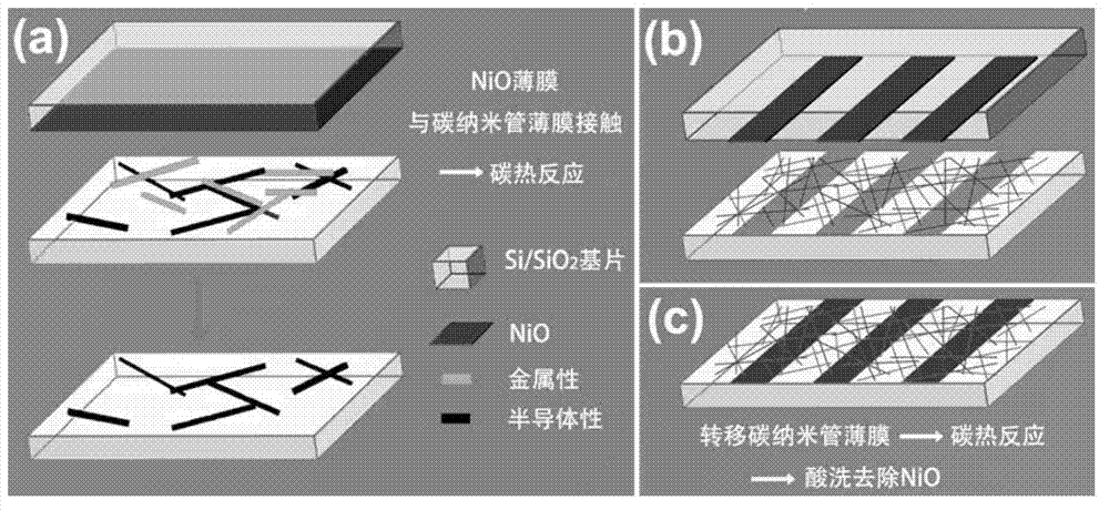
[0037] The invention provides a design and preparation method of a full single-wall carbon nanotube field effect transistor, which is prepared by low-temperature carbon-thermal reaction of metal oxides and photolithography technology, including the following steps:

[0038] (1) Using ion beam assisted deposition (IBAD) on Si / SiO 2 Substrate (Si substrate surface covered with a layer of amorphous SiO 2 , SiO 2 layer thickness of 100-500nm) SiO 2 Deposit 0.02-2nm thick catalyst (such as: Fe, Ni or Co, etc.) on the surface. The substrate after the deposition of the metal film is at 800-1000°C under Ar / H 2 (Ar, H 2 Mixed gas in any proportion. Preferably, by volume ratio, H 2 85~95%, Ar5~15%) pretreatment in the mixed atmosphere for 2-20min to form metal nanoparticles, and then use Ar to load hydrocarbon organic matter as a carbon source to trigger the growth of single-walled carbon nanotubes. Single-walled carbon nanotubes are The sample grows on the surface and exists in th...

Embodiment 1

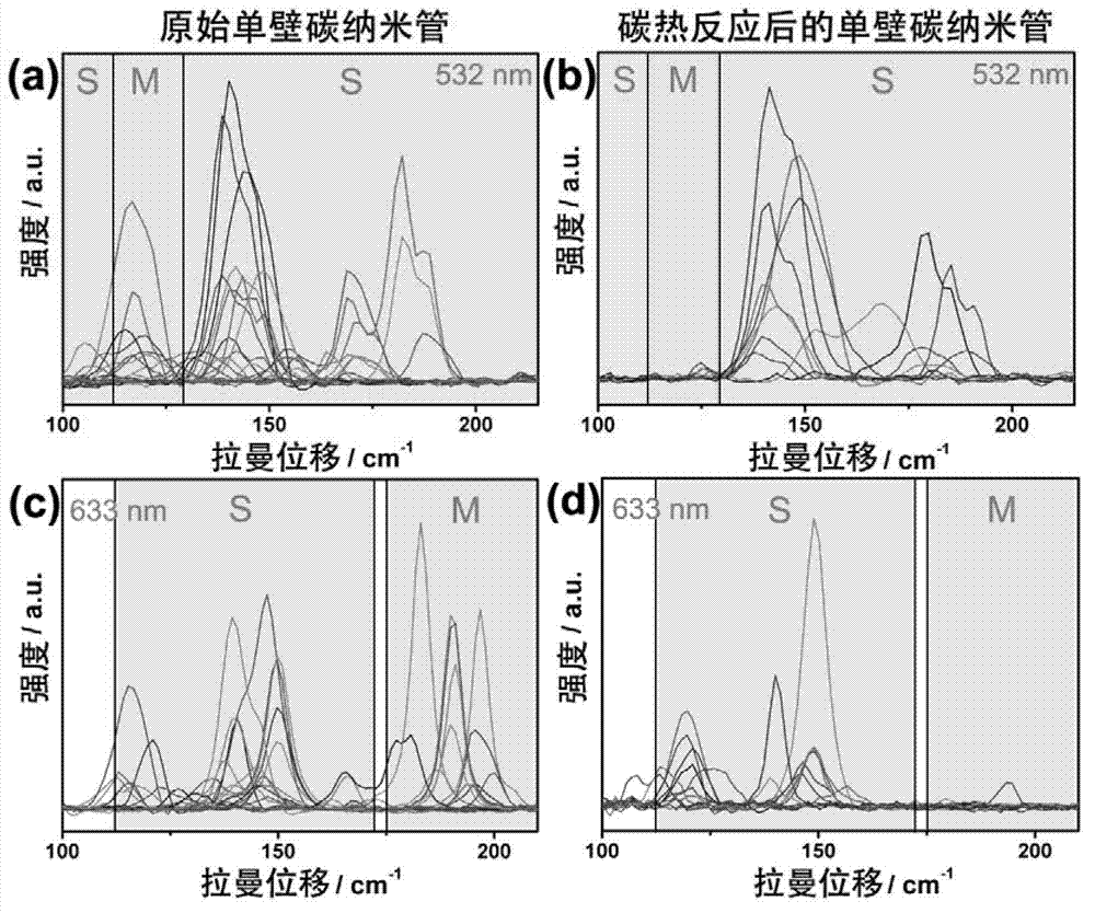
[0046] Si / SiO by ion beam assisted deposition 2 A 0.02 nm thick Co film was deposited on the substrate as a catalyst. The matrix is ​​at 950°C and Ar / H 2 (by volume ratio, H 2 90%, Ar 10%) in a mixed atmosphere for 5 minutes to form Co nanoparticles with a particle size of 1-5nm, and then use Ar to load C 2 h 5 OH was used as a carbon source to grow single-walled carbon nanotubes. Raman spectra of as-grown single-walled carbon nanotubes, such as figure 2 (a) and figure 2 (c) shown. Raman spectrum characterization shows that the obtained is a mixture of metallic and semiconducting carbon nanotubes.

[0047] On Si / SiO 2 A 100nm Ni film was deposited on the substrate and oxidized at 600°C. The substrate with NiO film and the substrate with single-walled carbon nanotube film are stacked against each other, and pressure is applied to ensure the tight fit between the two. After 30 minutes of carbon thermal reaction in an air atmosphere at 350°C, the two Separated, pickle...

Embodiment 2

[0049] Si / SiO by ion beam assisted deposition 2 A 0.1 nm thick Co film was deposited on the substrate as a catalyst. matrix at 900°C and Ar / H 2 (by volume ratio, H 2 50%, Ar 50%) in a mixed atmosphere for 10 minutes to form Co nanoparticles with a particle size of 1-5nm, and then use Ar to load C 2 h 5 OH was used as a carbon source to grow single-walled carbon nanotubes.

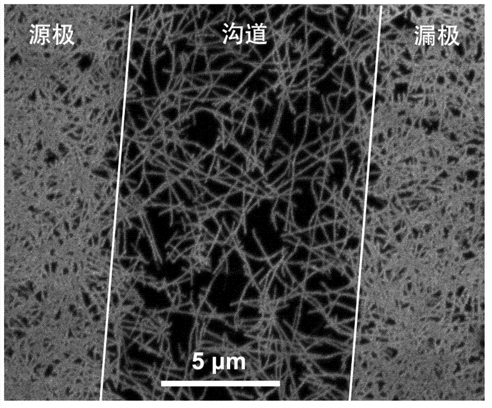
[0050] Si / SiO by photolithography 2 Ni lines are deposited on the substrate, the thickness of the Ni lines is about 100 nm, the width of the Ni lines is 10 μm, and the interval is 200 μm. The Ni lines were pre-oxidized to form NiO in an air atmosphere at 600 °C. After 30 minutes of carbon thermal reaction in an air atmosphere at 350°C, the two were separated, and the residual NiO was removed by pickling, and the NiO was washed and removed with 1M (mol / L) HCl solution, and the substrate was washed and dried with deionized water. , the preparation process is as figure 1 (c) shown. Only semiconducting...


PUM

PropertyMeasurementUnit
particle sizeaaaaaaaaaa
thicknessaaaaaaaaaa
widthaaaaaaaaaa

Abstract

The invention relates to the field of single-walled carbon nanotubes, in particular to an all-single-walled carbon nanotube field effect transistor and a preparation method thereof. Semiconductor single-walled carbon nanotubes are utilized as channels of field effect transistors, and metallic / semiconductor single-walled carbon nanotube mixtures are used as source and drain electrodes. Metallic oxide and the single-walled carbon nanotubes can be in carbon heat reaction at proper temperature, and high-chemical-activity metallic single-walled carbon nanotubes are selectively etched to obtain semiconductor single-walled carbon nanotubes. A metal film is deposited on a Si / SiO2 substrate by using photolithography, and is pre-oxidized to obtain a metallic oxide film. Only the semiconductor single-walled carbon nanotubes are reserved in the single-walled carbon nanotube film and a reaction region which is in contact with metal oxide and are used as the channels of the field effect transistors, and the single-walled carbon nanotubes which are unaffected and are positioned out of the channels are utilized as the source and drain electrodes. Metal electrodes are not required to be deposited; and the all-single-walled carbon nanotube field effect transistor can be used for flexible devices, has the characteristics of cleanness and high efficiency, and can be used for manufacturing large-scale all-carbon integrated circuits possibly.

Description

technical field [0001] The invention relates to the field of single-wall carbon nanotubes, in particular to an all-single-wall carbon nanotube field-effect transistor and a preparation method thereof. Background technique [0002] Single-walled carbon nanotubes have good application prospects in the next generation of nanoelectronic devices due to their excellent electrical, optical, and mechanical properties. For example, single-walled carbon nanotubes have a current-carrying density of up to 10 9 A / cm 2 , which is several orders of magnitude higher than the traditional metal material copper; field effect transistors constructed of semiconducting single-walled carbon nanotubes can achieve current regulation with a switching ratio of up to 10 by adjusting the gate voltage. 5 , is an ideal basic unit as a logic circuit. However, all SWNT preparation methods yield SWNTs that are a mixture of metallic and semiconducting properties. Usually, 1 / 3 of the product is metallic an...

Claims


Application Information

Patent Timeline
Patent Type & Authority Applications(China)
IPC IPC(8): H01L29/772H01L21/04B82Y10/00
Inventor 刘畅李世胜侯鹏翔成会明
Owner INST OF METAL RESEARCH - CHINESE ACAD OF SCI
Why Eureka
Try Eureka