Epitaxial structure for improving luminous efficiency and preparation method thereof

A technology of epitaxial structure and luminous efficiency, applied in the direction of electrical components, circuits, semiconductor devices, etc., can solve the problems of reduced luminous efficiency of quantum wells, uneven carrier distribution, huge built-in electric field, etc., to achieve optimal concentration distribution, Effect of improving luminous efficiency and reducing stress

Active Publication Date: 2015-07-22
宁波安芯美半导体有限公司
View PDF4 Cites 0 Cited by
  • Summary
  • Abstract
  • Description
  • Claims
  • Application Information

AI Technical Summary

Problems solved by technology

[0006] In view of the above-mentioned shortcomings of the prior art, the object of the present invention is to provide an epitaxial structure and a preparation method thereof for improving luminous efficiency, which are used to solve the huge built-in electric field and the The problem of reduced luminous efficiency of quantum wells caused by uneven carrier distribution

Method used


Image

  • Epitaxial structure for improving luminous efficiency and preparation method thereof
  • Epitaxial structure for improving luminous efficiency and preparation method thereof

Examples


Embodiment Construction

[0043] The following describes the implementation of the present invention through specific specific examples. Those skilled in the art can easily understand other advantages and effects of the present invention from the content disclosed in this specification. The present invention can also be implemented or applied through other different specific embodiments, and various details in this specification can also be modified or changed based on different viewpoints and applications without departing from the spirit of the present invention.

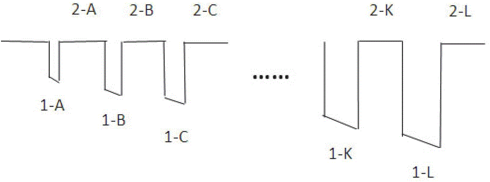
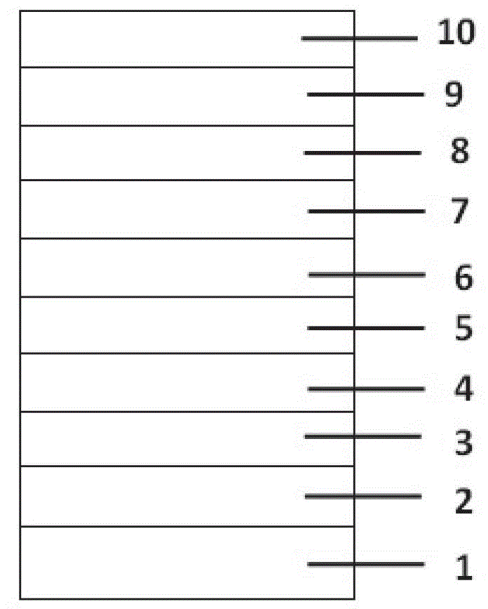
[0044] See Figure 1 to Figure 2 Shown. It should be noted that the illustrations provided in this embodiment only illustrate the basic idea of ​​the present invention in a schematic way, and the figures only show the components related to the present invention instead of the number, shape, and shape of the components in actual implementation. For size drawing, the type, quantity, and proportion of each component can be changed at will durin...


PUM


Abstract

The invention provides an epitaxial structure for improving luminous efficiency. The epitaxial structure for improving the luminous efficiency sequentially comprises a substrate, a first GaN (Gallium Nitride) buffer layer, a second GaN buffer layer, an N-type GaN layer, a multi-quantum well (MQW) structure, a light-emitting layer multi-quantum well structure, a p-type GaN layer, a p-type AlGaN (aluminium gallium nitride) layer, a p-type GaN layer and a p-type contact layer from the bottom up, wherein the multi-quantum well structure consists of n layers of InxGa1-XN / GaN multi-quantum wells; the widths, the depths and the barrier heights of the n layers of the multi-quantum wells increase layer by layer; the barrier widths of the n layers of the multi-quantum wells decrease layer by layer; the well widths increasing layer by layer and the barrier widths decreasing layer by layer form regular correspondence; and n is an integer in a range of 2-12. A preparation method of the epitaxial structure for improving the luminous efficiency can optimize concentration distribution of electrons, reduce stresses generated in growth processes of multi-quantum wells, reduce a quantum confined stark effect (QCSE) and improve the luminous efficiency of the multi-quantum wells.

Description

Technical field [0001] The invention belongs to the technical field of gallium nitride-based material preparation, and particularly relates to a method for improving the luminous efficiency of multiple quantum wells by a gallium nitride-based light-emitting diode. Background technique [0002] Group III nitride represented by gallium nitride is a wide bandgap semiconductor material with a direct band gap. It has high electron drift saturation speed, good thermal conductivity, radiation resistance, high temperature resistance, and good chemical stability and physical stability. The band gap of its ternary alloy indium gallium nitride (InGaN) is continuously adjustable from 0.7 eV indium nitrogen (InN) to 3.4 eV gallium nitride (GaN), and its emission wavelength covers the entire region of visible light and near ultraviolet light. Light-emitting diodes with InGaN / GaN multiple quantum wells as the active layer have outstanding characteristics such as high efficiency, environmental ...

Claims


Application Information

Patent Timeline
Patent Type & Authority Patents(China)
IPC IPC(8): H01L33/02H01L33/06
Inventor 郭丽彬王耀国钟伊泰
Owner 宁波安芯美半导体有限公司
Why Eureka
Try Eureka