Film heat flux sensor and preparation method thereof
A technology of heat flow sensor and thin film, which is applied to thermometers, instruments, scientific instruments, etc. that are directly sensitive to heat, electric/magnetic components, etc., can solve the problems of slow response time and large volume, so as to improve the reliability level and realize batch production Production, the effect of reducing manufacturing costs
- Summary
- Abstract
- Description
- Claims
- Application Information
AI Technical Summary
Problems solved by technology
Method used
Image
Examples
Embodiment 1
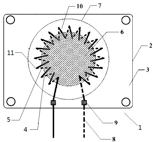
[0036] see figure 1 , the thin film heat flow sensor 1 comprises a substrate 2, a transition layer 3 disposed on the substrate 2, a thin film thermocouple array disposed on the transition layer 3; the thin film thermocouple array consists of more than two A electrodes 4 and The thin-film thermocouple 10 of the B electrode 5 is formed in series through the external contact 11; the contact of the A electrode 4 and the B electrode 5 is provided with a thick thermal barrier layer 6; the external contact 11 is provided with a thin thermal barrier layer 7; The two external ends of the two or more thin-film thermocouples 10 connected in series are respectively connected to the corresponding compensation wires 8 via a pad 9 (see figure 1 ).
[0037] Wherein, the material of the substrate 2 is Al 2 o 3 Ceramics, the diameter of which is 50 mm to 150 mm and the thickness of 0.5 mm to 1 mm; the material of the transition layer 3 is Ta 2 o 5 , with a thickness of 0.05 μm to 0.1 μm; t...
Embodiment 2
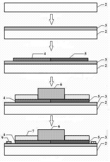
[0039] see figure 2 , the preparation method of the thin film heat flow sensor comprises the following steps:
[0040] (1) For Al with a diameter of 50mm to 150mm and a thickness of 0.5mm to 1mm 2 o 3 The substrate is cleaned to remove oil and impurities on the polished surface of the substrate;
[0041] (2) Set the substrate and the stainless steel mask of the R-type PtRh13-Pt thermocouple PtRh13 electrode together, and clamp it with a stainless steel fixture and put it on the planet carrier of the ion beam sputtering coating machine;
[0042] (3) Deposit Ta with a thickness of 0.05 μm to 0.1 μm by ion beam sputtering 2 o 5 Transition film and PtRh13 thermocouple thin film of 0.1 μm ~ 0.2 μm, remove the stainless steel mask;
[0043] (4) Set the substrate and the stainless steel mask of the R-type PtRh13-Pt thermocouple Pt electrode together, and clamp it with a stainless steel fixture and put it on the planet carrier of the ion beam sputtering coating machine;
[0044...
PUM
| Property | Measurement | Unit |
|---|---|---|
| diameter | aaaaa | aaaaa |
| thickness | aaaaa | aaaaa |
| thickness | aaaaa | aaaaa |
Abstract
Description
Claims
Application Information

