III-V group semiconductor MOS field effect transistor with high mobility

A field effect transistor, III-V technology, applied in semiconductor devices, electrical components, circuits, etc., can solve the problems of increasing the equivalent oxide layer thickness of MOS devices, etc., to reduce scattering, low interface state density, and improve driving current. Effect

Inactive Publication Date: 2013-02-13
INST OF MICROELECTRONICS CHINESE ACAD OF SCI
View PDF5 Cites 26 Cited by
  • Summary
  • Abstract
  • Description
  • Claims
  • Application Information

AI Technical Summary

Problems solved by technology

However, due to the addition of the barrier layer, the equivalent oxide thickness of the MOS device is increased, and the parasitic resistance of the source and drain of the MOS device is increased, which limits the improvement of the driving current and switching speed of the device to a certain extent.

Method used


Image

  • III-V group semiconductor MOS field effect transistor with high mobility
  • III-V group semiconductor MOS field effect transistor with high mobility

Examples


Embodiment Construction

[0032] In order to make the object, technical solution and advantages of the present invention clearer, the present invention will be described in further detail below in conjunction with specific embodiments and with reference to the accompanying drawings.

[0033] The MOS field effect transistor with a doped interface control layer provided by the present invention uses the interface control layer to reduce the scattering of carriers in the channel to achieve high effective channel mobility; The method of doping with the interface control layer can increase the carrier concentration in the channel layer, thereby increasing the driving current of the device.

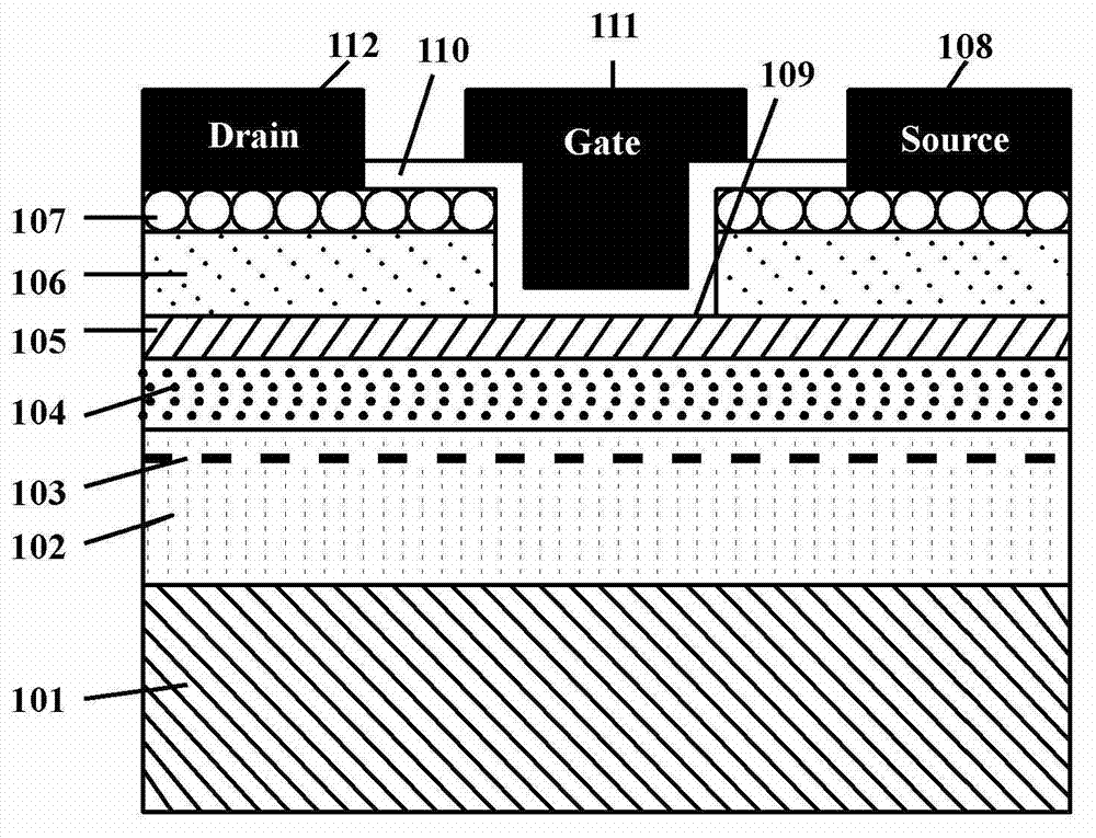
[0034] Such as figure 1 as shown, figure 1 It is a schematic structural diagram of a high mobility III-V semiconductor MOS field effect transistor according to an embodiment of the present invention, and the field effect transistor includes: a single crystal substrate 101; a buffer layer 102 formed on the single crysta...


PUM


Abstract

The invention discloses a III-V group MOS (Metal-oxide Semiconductor) field effect transistor with high mobility, which comprises a single-crystal lining, a buffer layer formed on the single-crystal lining, a planar doped layer formed in the buffer layer, a high-mobility channel layer formed on the buffer layer, a doped interface control layer formed on the high-mobility channel layer, a high-doped semiconductor layer formed on the doped interface control layer, a narrow band gap ohm contact layer formed on the high-doped semiconductor layer, and a source-drain metal electrode formed on the narrow band gap ohm contact layer, wherein a grid groove etched to the doped interface control layer is located between two source drain metal electrodes; a high-K grid medium is uniformly covered on the inner surface of the grid groove structure; and a grid metal electrode is formed on the high-K grid medium. The III-V MOS device structure disclosed by the invention not only can lower MOS interface state density, and improve channel mobility, but also can improve channel two-dimensional electron (cavity) gas concentration, and satisfy the application demand of a high-speed lower voltage operation high mobility CMOS technology.

Description

technical field [0001] The invention relates to the technical field of semiconductor integrated circuit manufacturing, in particular to a high-mobility III-V group that achieves high drive current and low source-drain resistance by doping an interface control layer, planar doping, and heavily doped source-drain technology. The semiconductor metal oxide semiconductor (MOS) field effect transistor can be applied to high-performance III-V MOS devices and circuits. Background technique [0002] After silicon-based complementary metal oxide semiconductor (CMOS) technology enters the 22nm technology node, it is difficult to improve device performance by scaling down. Using new materials and new devices has become an important research direction to continue to improve the performance of CMOS devices. III-V semiconductor materials have become a hot topic in current research due to their excellent electron transport properties. However, due to the high interface state density of III...

Claims


Application Information

Patent Timeline
Patent Type & Authority Applications(China)
IPC IPC(8): H01L29/778H01L29/78H01L29/06
Inventor 刘洪刚常虎东薛百清王虹刘桂明
Owner INST OF MICROELECTRONICS CHINESE ACAD OF SCI
Why Eureka
Try Eureka