Luminous display back plane, method for preparing pixel definition layer thereof and display device

A pixel-defining layer and light-emitting display technology, applied in lighting devices, optomechanical equipment, electroluminescent light sources, etc., can solve the problems of increasing the number of masks used, increasing the exposure process, and unfavorable mass production

Inactive Publication Date: 2013-03-13
BOE TECH GRP CO LTD
View PDF5 Cites 28 Cited by
  • Summary
  • Abstract
  • Description
  • Claims
  • Application Information

AI Technical Summary

Problems solved by technology

[0005] The second type is currently inclined to use a double-layer film structure to form an inverted trapezoidal pixel definition layer (PDL), but this solution

Method used


Image

  • Luminous display back plane, method for preparing pixel definition layer thereof and display device
  • Luminous display back plane, method for preparing pixel definition layer thereof and display device
  • Luminous display back plane, method for preparing pixel definition layer thereof and display device

Examples


Embodiment 1

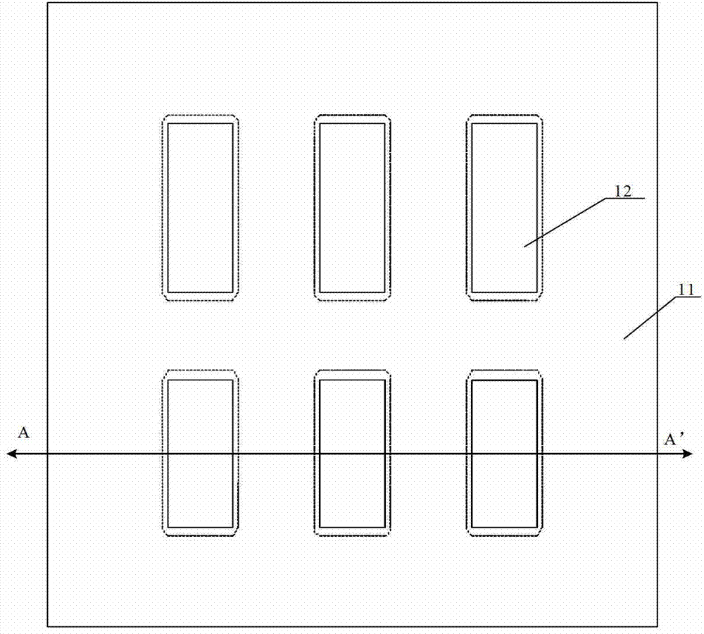
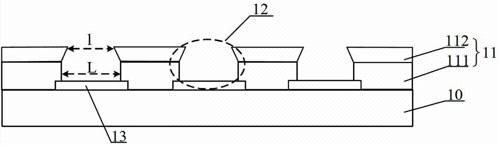
[0045] An embodiment of the present invention provides a light-emitting display backplane, such as figure 1 and figure 2 As shown, the backplane includes: a substrate 10 and a pixel defining layer 11 disposed on the substrate 10, and the pixel defining layer 11 includes:

[0046] A photosensitive resin layer 111 and a transparent boundary layer 112 arranged sequentially from bottom to top;

[0047] The photosensitive resin layer 111 and the transparent delimiting layer 112 are provided with openings in corresponding regions of each pixel, and the openings of the transparent delimiting layer 112 are smaller than the openings of the photosensitive resin layer 111, so as to form a luminescent material filling domain 12 that is wide at the bottom and narrow at the top. .

[0048] The light-emitting display backplane includes a substrate, an ITO (Indium Tin Oxide, indium tin oxide) anode, a light-emitting layer, a cathode, and the like. Among them, when forming the light-emitti...

Embodiment 2

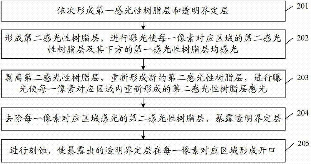
[0058] An embodiment of the present invention provides a method for preparing a pixel defining layer of a light-emitting display backplane. The light-emitting display backplane includes: a substrate and a pixel defining layer disposed on the substrate, such as image 3 As shown, the method includes:

[0059] Step 201, sequentially forming the photosensitive resin layer 111 and the transparent boundary layer 112, such as Figure 4 shown;

[0060] This step forms the lowermost photosensitive resin 111 and the transparent defining layer 112 on it, and the way to form (or prepare) these film layers can be physical vapor deposition (PVD) methods such as evaporation, sputtering, ion plating, etc. It may also be a chemical vapor deposition (CVD) method, generally selected according to the material of the film to be deposited, which is not limited in this embodiment. Taking the transparent defining layer 112 as an example of a silicon nitride film, a specific preparation scheme is a...


PUM


Abstract

The invention discloses a luminous display back plane, a method for preparing a pixel definition layer thereof and a display device and relates to the field of display. The luminous material drops formed in printing can be laid in a pixel area of the pixel definition layer and cannot flow to the adjacent pixel area. The luminous display back plane comprises a substrate and the pixel definition layer arranged on the substrate, the pixel definition layer comprises a phototonus resin layer and a transparent definition layer, the phototonus resin layer and the transparent definition layer are arranged from bottom to top, openings are arranged on the corresponding area of every pixel of the phototonus resin layer and the transparent definition layer, the opening of the transparent definition layer is less than that of the phototonus resin layer, and a luminous material filling region which is narrow on the upper portion and wide on the lower portion is formed.

Description

technical field [0001] The invention relates to the field of display, in particular to a method for preparing a luminescent display backplane and a pixel defining layer thereof, and a display device provided with the luminescent display backplane. Background technique [0002] Organic light emitting display (Organic Light Emitting Diode, OLED) display has self-illumination, no backlight, high contrast, thin thickness, wide viewing angle, fast response, can be used for flexible panels, wide operating temperature range, structure It is considered to be an emerging technology for the next generation of flat panel displays due to its excellent characteristics such as simple manufacturing process. [0003] The OLED display backplane includes a substrate, an ITO (Indium Tin Oxide, indium tin oxide) anode, a light-emitting layer, and a cathode. On the band, a photon with the same energy as the energy gap is released, and its wavelength (luminescent color) depends on the energy gap...

Claims


Application Information

Patent Timeline
IPC IPC(8): H01L27/32H01L51/52H01L51/56
CPCG02F1/1335G02F1/133516G03F7/0007H05B33/10
Inventor 姜春生
Owner BOE TECH GRP CO LTD
Why Eureka
Try Eureka